|
Theoretical investigations on MOS structures have already been addressed by numerical simulations within a semi-classical treatment. Due to the strong impact of quantum mechanical effects on MOS inversion layers, the effects of quantization are taken into account through the treatment of two-dimensional subband states. This is highly problematic in the case of accumulation layers, because in addition to the discrete states, there is also the non-negligible contribution of the continuum states. A more rigorous investigation achieved through the application of the Non-Equilibrium Green's Functions (NEGF) formalism is not affected by this problem and yields the current directly. Previously developed, adaptive numerical quadrature methods have been applied to correctly resolve the narrow resonant states in the energy spectrum. The influence of level broadening due to scattering processes has been modeled by means of an optical potential. The gate and the bulk regions have been assumed to be in thermal equilibrium and are characterized by Fermi energies.
The new model developed here allows an equal treatment of the Quasi-Bound States (QBS) within the channel and the continuum. Hence, the effects of the QBS on the electrostatics and the current spectrum are treated simultaneously and in a consistent manner.
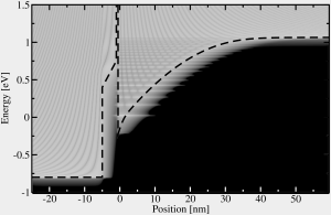
The NEGF approach gives rise to distinct resonant states within the density of states, as depicted in the figure. In contrast to the closed boundary model, these peaks show a realistic broadening due to the scattering processes modeled according to the optical potential. On the other hand, the semi-classical treatment completely neglects the resonances. This demonstrates that the closed boundary and the semi-classical model capture only the extreme cases of a quantized system and free electron gas, respectively.
|