Erasmus Langer
Siegfried Selberherr
Oskar Baumgartner
Hajdin Ceric
Johann Cervenka
Otmar Ertl
Wolfgang Gös
Klaus-Tibor Grasser
Philipp Hehenberger
René Heinzl
Gerhard Karlowatz
Markus Karner
Hans Kosina
Gregor Meller
Goran Milovanovic
Mihail Nedjalkov
Roberto Orio
Vassil Palankovski
Mahdi Pourfath
Franz Schanovsky
Philipp Schwaha
Franz Stimpfl
Viktor Sverdlov
Oliver Triebl
Stanislav Tyaginov
Martin-Thomas Vasicek
Stanislav Vitanov
Paul-Jürgen Wagner
Thomas Windbacher

Vassil Palankovski
Dipl.-Ing. Dr.techn.
palankovski(!at)iue.tuwien.ac.at
Biography:
Vassil Palankovski was born in Sofia, Bulgaria, in 1969. He received the diploma degree in electronics from the Technical University of Sofia in 1993. Afterwards he worked for three years in the telecommunications field. In March 1997, he joined the Institute for Microelectronics at the Technische Universtität Wien, where he received his doctoral degree in technical sciences in 2000 and continued as a post-doctoral researcher. In summer 2000, he held a visiting research position at LSI Logic Corporation, Milpitas, California. In 2003, Dr. Palankovski and Dr. Quay published the book Analysis and Simulation of Heterostructure Devices in the Springer Series on Computational Microelectronics. In 2004, he joined Infineon Technologies, Villach, Austria, for half a year as a technology development engineer. Having received the highest Austrian award for young scientists (START-Prize), Dr. Palankovski returned to the Technische Universität Wien in 2005 to establish the Advanced Materials and Device Analysis group. In 2008, he was elected a member of the young curia of the Austrian Academy of Sciences.

Analysis and Simulation of Advanced Heterostructure Devices

A large project (START) on the "Simulation of Advanced Semiconductor Devices" funded by the Austrian Federal Ministry for Science and Research (BMWF) through the Austrian Science Fund (FWF) has entered its fourth year.
The project includes several research topics, such as the modeling of novel semiconductors (strained Si/SiGe, various III-Vs, as well as the Group IV-VI material systems). The device applications include advanced high-frequency high-power Heterojunction Bipolar Transistors (HBTs) and High Electron Mobility Transistors (HEMTs), as well as quantum wires and high-efficiency solar cells.
The physical material properties are characterized for wide ranges of material compositions, temperatures, doping concentrations, etc. by means of a Monte Carlo (MC) simulation. A new 2D Ensemble Monte Carlo code was developed and verified versus a bulk MC code for different materials. It is being used as a platform for the development of a 2D Wigner quantum MC code.
Physics-based analytical models for the lattice, thermal, band structure, and transport properties of various semiconductor materials, as well as models for important high-field and high-doping effects taking place in the devices, are derived and implemented in the device simulator Minimos-NT. The models are calibrated against experimental data from our scientific partners. Novel device structures are investigated, designed, and optimized.
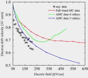
For example, a recent work on "Negative differential mobility at ultrahigh fields: comparison between an experiment and simulations" (APL 92, 062114, 2008) explains that the superfast switching observed in GaAs bipolar transistors should take place only with a strong negative differential electron mobility up to an electric field of 600 kV/cm. A satisfactory velocity-field dependence is predicted only by our 3-valley MC simulations.


Electron velocity vs. electric field in GaAs: Comparison of different Monte Carlo approaches.


Home | Activities | Staff | Publications | Sponsors | Contact Us