|
In the design of high-performance semiconductor devices strain technology takes a key position among other technological innovations due to its cost effectiveness and the beneficial effect of strain on device performance. Strain alters the shape of the valence band structure affecting the effective mass and mobility. The symmetry of the band structure is reduced and the bands are shifted in energy by an amount related to the strain. We present an analytical expression for the deformation potential operator; in addition, it was possible to show that the potential part satisfies a Fredholm integral equation of the second kind. Due to the orthonormality of the eigenfunctions, the solution can be written as an expansion in reciprocal lattice vectors with coefficients depending on the transformation of the atomic basis vector. The method does not make use of the internal strain parameter, which was introduced by Kleinman in order to specify the position of the atom in the strained
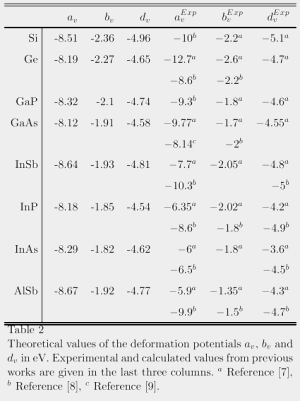
lattice. The measurement of the internal strain parameter is rather difficult and only few experimental data are available; not all are in agreement with one another. We fix the strained atomic basis vector by means of the measured deformation potentials of GaSb. Having determined the transformation of the atomic basis vector, theoretical values for the valence band deformation potentials are calculated for the semiconductors: Si, Ge, GaP, GaAs, InSb, InP, InAs and AlSb. Our calculation features a new method of avoiding problems arising from the internal strain parameter. Once the transformation of the atomic basis vector is fixed, it can be applied to all semiconductors of diamond and zincblende structures.
|