|
Electromigration can trigger system failure at an undefined time in future and is the main reliability issue in modern integrated circuits. An accurate simulation of the vacancy distribution is necessary to simulate this behavior. It is in this context that electrical current, temperature distribution, and mechanical stress have to be calculated. Finite element methods on tetrahedral meshes are used to compute the coupled electro-mechanical system. Particularly in dual-damascene copper interconnects, totally different vacancy distributions can be observed when the copper grains are taken into account. The network of grain boundaries influences the vacancy transport during electromigration severely.
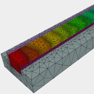
Due to the necessity to produce such grains in the copper interconnect, existing layout and mesh modules have been extended. Based on a given geometry, different grain sizes with adjustable variances in the size and direction of the grain boundaries can be inserted automatically in this primary structure. A crucial aspect of this procedure is the required mesh generation. In order to accurately solve the stress calculation, the mesh must resolve the thin layers properly, and the mesh densities must be dense around the material interfaces, which are the copper-barrier, copper-capping, and the copper-copper interfaces themselves. On the other hand, the total number of mesh points has to be low in order to achieve small system matrices. As the NETGEN mesher produces meshes with the desired requirements, an interface to this mesher has been developed. Following the mesh generation, its output has to be converted to a representation suitable for the finite element module which calculates the vacancy concentration. The figure depicts the interior of a typical dual-damascene test structure. Surrounding layers are partially cut away to release the pure copper.
|