|
Modern microelectronics demand the development of smaller and smaller transistor elements. Considering the modern MOSFET, this tendency presumes, among other things, the reduction of the gate oxide thickness which now lies in the range of less than 3 nm. This results in significant leakage currents through the gate. In spite of an impressive progress of silicon technology the fluctuations in the MOSFET parameters can never be removed. The impact of statistical variations of such parameters as doping concentration in the channel, its effective length, oxide thickness etc. on MOSFET output characteristics has been repeatedly raised in the literature, and it is quite obvious that the influence of the oxide thickness non-uniformity substantially increases when device dimensions shrink.
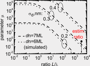
Besides its nominal thickness, the insulator layer in a MOS device is characterized by the standard deviation which is a measure of the non-uniformity of the thickness distribution throughout the device area. Thereby we distinguish between the local and the nominal thickness. The local thickness is assumed to be a statistical quantity that obeys the Gaussian distribution with the mean value equal to the nominal thickness and corresponding standard deviation. It is clear that the spatial fluctuations of the insulator thickness cannot occur arbitrarily abruptly. To account for this, the correlation length of thickness variations is introduced, which is to be understood as a minimal distance between two points, whereby the local thicknesses are taken to be independent. This length, like the standard deviation of the insulator thickness, is the overall quality indicator for a dielectric layer. Practically, the correlation length should be small with respect to the device dimensions.
A novel technique for experimental estimation of the correlation length of insulator thickness fluctuations is proposed which is based on the statistical treatment of spread of current densities in a random set of devices. This technique has been quite successfully examined using two very different types of samples, namely Al/SiO2/Si diodes with large (to reinforce all the effects) oxide thickness deviations, as well as Au/CaF2/n-Si(111) structures with an epitaxial fluoride layer. In both cases, satisfactory agreement was achieved with results on correlation lengths yielded by a direct measurement of the same fluoride or oxide layers with an atomic force microscope. An advantage of the proposed method is its simplicity as it does not rely on microscopy-aided diagnostics. However, the accuracy of our method will be insufficient for very small thickness dispersion, which is just the case in modern technology of field-effect transistors. For this reason, the new method is potentially more interesting and useful for tunnel-thin films of insulating materials for which the overall technology level is inferior to that of SiO2. This, however, is just the case on the current search for alternative dielectrics (e.g. high-K gate insulators).
|