|
Advances in microelectronics have led to the aggressive scaling of device geometries causing the emergence of reliability issues, such as Negative Bias Temperature Instability (NBTI), Hot Carrier Injection (HCI), and Time-Dependent Dielectric Breakdown (TDDB). The origins of these reliability concerns still pose riddle and are strongly debated. In this context, charge trapping is frequently suspected to account for a crucial contribution to HCI and NBTI. Particularly in the NBTI literature, hole trapping is held responsible for either the fast or the slow component. To clarify this unsettled issue, a detailed investigation is of outmost importance. Until now, Tewksbury's model has appeared to rest on a sound foundation. However, its limitations become more and more apparent as ever thinner dielectrics are encountered. In this model, charge trapping is restricted to charge injection from the substrate and ignores the presence of the gate contact as a source or a sink of charge carriers. An extension of this model to account for the gate contact reveals considerably shorter tunneling times.
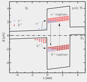
Recent first-principle investigations on defects in the dielectric indicate distinct trap levels for different defect charge states — a fact that has not been respected so far. This novel picture of tunneling into and out of defects can be envisioned by level shifts as illustrated in the figure. It originates from an atomic relaxation of the defect configuration and alternating energetics giving rise to the aforementioned level shift. Furthermore, it questions the conventional concept of fixed trap levels, irrespective of their charge state. These level shifts have been rigorously incorporated into a new model. Numerical simulations have been performed on top of a Schröderinger-Poisson solver and yield a new transient behavior, which spans over decades as observed in the experiments. Moreover, the transient behavior for each trap shows a charging-up behavior attributable to strong favoring for either trapping or detrapping. The spatial spread of traps, as well as the spread of energy, entails the superposition of a large number of single trapping processes with different tunneling times. This gives rise to new features not observed within the framework of conventional trapping models. In the light of this novel model, NBTI and HCI are reexamined.
|