|
Since electromigration has been recognized as an important risk for
interconnect reliability, engineers have been searching for strategies to
reduce or completely eliminate its effects. Independent of
interconnect technology, there are basically two possible ways how to
contest electromigration. The first one is choosing the appropriate
materials or combination of these materials to produce preferable
properties. Such efforts led from originally aluminum interconnects to
aluminum-copper alloys, and later to pure copper interconnects. This method of designing
interconnect structures to increase reliability also encompasses choosing the materials
that surround the interconnect metal. The second strategy for the control of
electromigration behavior is the introduction of special geometrical
features. The basic idea is to avoid dwindling material due to material
transport in specific interconnect structures. The most widely applied
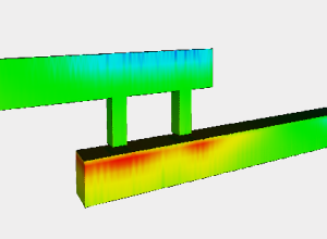
examples of such strategies are material reservoirs and redundant vias.
Using two or more via contacts between interconnect levels has proven to
be a very promising geometrical strategy for preventing
electromigration. This is because the nucleation of a void underneath
the first via is supposed to relax the stress under the second one as well,
suppressing the driving force for the formation of a new void.
Most recently, the electromigration model has been implemented in
the Finite Element Diffusion and Oxidation Simulator (FEDOS) for three-dimensional
geometries. All important driving forces have been taken into account in
the vacancy transport equation. Furthermore, anisotropic material transport
generated by the stress has also been implemented. Fast diffusivity
paths for material transport, such as grain boundaries and material
interfaces, have also been included in the model, allowing the study of
the impact of each individual path on the electromigration phenomenon.
|