Chapter 5
Pulsed BTI Measurements
In the previous chapter various BTI stress tests were performed using the
measurement-stress-measurement (MSM) and the on-the-fly (OTF) technique.
Special attention was given to the fitting of the measurement data onto a
universal relaxation law, yielding a separation of the degradation into a
recoverable and a poorly recoverable or permanent component. Data gathered at
different temperatures and stress voltages were found to follow a universal
relaxation law. Interestingly both stress polarities, i.e. NBTI and PBTI stress on
a pMOS, always resulted in a negative shift of the threshold voltage.
Unfortunately, PBTI had been rarely discussed in literature until Liu et al.
monitored a positive shift of the threshold voltage due to PBTI-stressed
pMOS-devices [24], which contradicts the results presented by Grasser et al.
[30].
One reason of this discrepancy might be the fact that Grasser et al. used the
OTF and the eMSM technique (cf. Chapter 2.3 and 2.1.3), while the two
measurement techniques used in [24] are both based on the application of fast
gate pulses: The newly developed on-the-fly fast charge pumping (OFIT)
technique and the fast pulsed  -characteristics have been discussed in
Chapter 2.5 and 2.2.1. The measurement results obtained by those two pulsed
setups are only at a first glance interpreted in a correct way, as the
-characteristics have been discussed in
Chapter 2.5 and 2.2.1. The measurement results obtained by those two pulsed
setups are only at a first glance interpreted in a correct way, as the  -curve
obtained by OFIT is simply scaled to align the
-curve
obtained by OFIT is simply scaled to align the  -curve at the end of
the recovery phase in [24]. Based on this alignment scheme depicted in
Fig. 5.1 and Fig. 5.2, Liu et al. stated a fast oxide trap component (
-curve at the end of
the recovery phase in [24]. Based on this alignment scheme depicted in
Fig. 5.1 and Fig. 5.2, Liu et al. stated a fast oxide trap component ( )
corresponding to the difference of
)
corresponding to the difference of  , which is
shown in the insets of Fig. 5.1 and Fig. 5.2. Compared to that, the interface
states are considered to recover only slowly. It was furthermore concluded
that the fast oxide traps are responsible for the predominant part of
, which is
shown in the insets of Fig. 5.1 and Fig. 5.2. Compared to that, the interface
states are considered to recover only slowly. It was furthermore concluded
that the fast oxide traps are responsible for the predominant part of
 -degradation in the fast pulsed
  -characteristics only, since their
influence during a DC measurement is drastically reduced due to the
measurement delay. Consequently, this makes the interface states dominate the
DC regime.
-characteristics only, since their
influence during a DC measurement is drastically reduced due to the
measurement delay. Consequently, this makes the interface states dominate the
DC regime.
When taking a closer look at the pulsed  -characteristics of Fig. 5.1
and Fig. 5.2, a surprisingly huge offset of about
-characteristics of Fig. 5.1
and Fig. 5.2, a surprisingly huge offset of about  between the reference
value and the first measurement point after
between the reference
value and the first measurement point after  of stress can be detected. As
this already accounts for more than
of stress can be detected. As
this already accounts for more than  of the total degradation built
up after
of the total degradation built
up after  of stress, the high initial
  seems to be at least
questionable.
seems to be at least
questionable.
In order to determine to what extent interface states and oxide charges really
contribute to the measurement signal, a more detailed study of the fast pulsed
 and the OFIT technique, besides further measurements is needed.
Especially the measurement delay of the setup in combination with its accuracy
is of particular interest here.
and the OFIT technique, besides further measurements is needed.
Especially the measurement delay of the setup in combination with its accuracy
is of particular interest here.
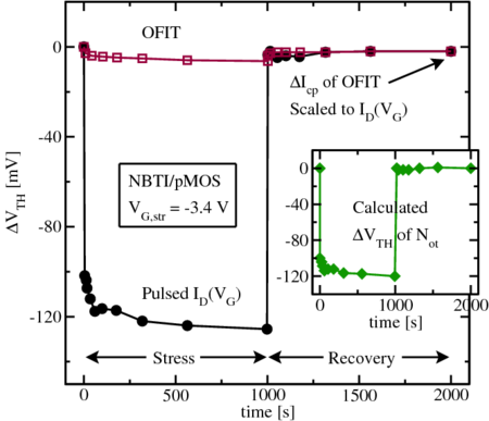
 of NBTI stress followed
by
of NBTI stress followed
by  of relaxation. While
  is measured by the FPM (open
squares),
is measured by the FPM (open
squares),  is measured by OFIT (solid circles). The fast pulsed
 -characteristics reveal a negative shift of
  for NBTI, while
during PBTI a positive shift is visible (Fig. 5.2). At the end of the recovery
phase the
for NBTI, while
during PBTI a positive shift is visible (Fig. 5.2). At the end of the recovery
phase the  curve is scaled to match the value of
  . According
to Liu et al. the difference between two curves (shown in the inset) yields
the amount of contributing oxide traps. Data is taken from [24].
. According
to Liu et al. the difference between two curves (shown in the inset) yields
the amount of contributing oxide traps. Data is taken from [24]. 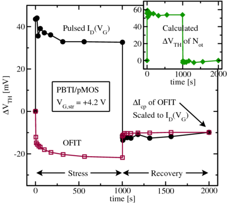
 of PBTI stress followed by
 of relaxation. While
  is measured by the FPM (open squares),
 is measured by OFIT (solid circles). In contrast to Fig.
  -characteristics reveal a positive shift of
  for PBTI. At
the end of the recovery phase the
for PBTI. At
the end of the recovery phase the  curve is scaled to match the value
of
curve is scaled to match the value
of  . According to Liu
  -Characteristics