Semiconductor devices are omnipresent in today’s everyday life. Phones have become high performance computers, there are microchips in almost all objects of daily use ranging from cars to bicycles, from washing machines to
fridges, and having microelectronic sensors and life preserving devices implanted in humans cannot be considered unusual anymore. This abundance of semiconductor technology in our lives has been made possible by the
decades-long, continuous miniaturisation of electrical circuits in accordance with Moore’s Law [1]. The invention of the bipolar junction transistor (BJT) in 1948 [2] and the monolithic silicon integrated circuit (IC) in 1959 [3] paved
the way for decades of ever smaller electronic devices shaping modern society. Also in 1959, the metal-oxide-semiconductor field-effect transistor (MOSFET) was invented and led to the transistor becoming the most frequently
fabricated object in human history [4]. For decades, MOSFET design did not change drastically [5], while its size could be decreased due to improved fabrication techniques, such as more focused lithography processes thanks to
better optics [6]. Lower power consumption and faster switching times, and thereby improved performance, were achieved through smaller dimensions and thinner insulating layers, meaning that smaller concentrations of electrical
charges were required for switching. However, starting in the early 2000 s, new fabrication techniques, such as strain engineering [7], new materials [8] and three-dimensional (3D) geometries [9] became essential to keep
improving upon the previous scaling processes. Nowadays, processors made of billions of single transistors contain numerous different materials in complex 3D arrangements, fabricated in meticulously calibrated steps performed at
highly stable temperatures, pressures and gas concentrations for well-defined time periods.
The required reliability and reproducibility of the complex fabricated structures made it necessary to develop physical models of devices and their operation from the beginning of transistor fabrication [10]. Starting in the
1960 s, the simulation of complex models on computers was becoming increasingly important in order to improve the understanding of the underlying physical processes at play and to increase the quality of the fabricated
devices [11]. As the fabrication techniques and the produced devices became more complex, so did their modelling and simulation approaches. By the 1970 s, modelling the fabrication and operation of semiconductor
devices, referred to as technology computer aided design (TCAD), had become an essential and widely used tool for manufacturers. This trend was only accelerated in later years and proper modelling is now crucial in all areas of
microelectronic device development, including fabrication, circuit design, as well as operation and long-time reliability. The inclusion of technological effects in the manufacture has become especially important, leading to several
advances in design technology co-optimisation (DTCO), which relies heavily on TCAD.
In order to better separate the wide range of modelling approaches, the simulation of fabrication steps such as etching, deposition, ion implantation and oxidation is referred to as process TCAD, while the simulation of the electrical
characteristics of the fabricated devices is referred to as device TCAD [12, 13]. In a modern DTCO cycle, the results of process TCAD are used in device TCAD to generate accurate descriptions of single devices, which are then
used in circuit TCAD to simulate their interaction in large electronic circuits. In this way, entire processors can be simulated to ensure that their desired functionality and reliability are achieved [14].
As process TCAD is the first step in modern development cycles, it is crucial that process-induced effects are well understood in order to ensure the reliable manufacture of modern devices and circuits. Due to the ever smaller sizes,
even small process deviations may lead to the catastrophic failure of components. Therefore, meaningful descriptions of each process step are critical for the correct prediction of the resulting fabricated structure.
Additionally, the fast development cycle of modern processors requires that large circuits and the potential interference of devices spaced closely on a microchip can be described in short time frames. Hence, the computational
efficiency of fundamental simulation methods, as well as process models, is key for modern microelectronic device development.
Therefore, the main focus of this work is centred on process TCAD. Specifically, the physical description of several different deposition and etching processes is considered, sometimes referred to as topography simulation.
Fundamental simulation concepts for the description of these process steps, as well as intricate physical models are developed and applied to advanced device structures. In order to meet the requirements of time-limited DTCO
development cycles, efficient approximations of these models are developed to allow for the fast evaluation of new circuit designs.
In this chapter, a general process flow for semiconductor fabrication is presented, highlighting the main steps this work will focus on, followed by the motivation and goals of this research, and an outline of the thesis.
1.1 Semiconductor Fabrication Process Flow
The fabrication of semiconductor devices consists of many steps which must produce well-defined structures with little deviations from one device to the next. Previous and subsequent fabrication steps must be taken into account at
every step to ensure the required high fabrication quality is achieved. Most processes are carried out in vacuum chambers by introducing different gaseous chemicals, which modify the surface by reacting with the substrate. The
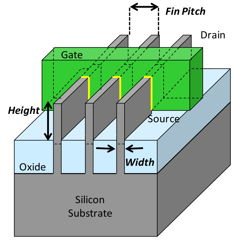
formation of the smallest features of an IC is referred to as front-end of line (FEOL) [15], which most of this work will focus on. The most important process steps during FEOL fabrication are explained in the following, using the
process flow of the 22 nm technology node for the fabrication of the FinFET shown in Fig. 1.1.
Illustrations of the most important fabrication steps are shown in Fig. 1.2. In-depth descriptions of how each of these steps can be modelled will be presented in Chapter 5. The FEOL steps of the fabrication of a FinFET usually are similar to the following:
1. The process initiates with a cleaned and polished crystalline silicon wafer.
2. Photolithography: In order to form the future conducting channel, i.e. the fin, a mask is created using photolithography, whereby only certain regions of the waver are covered by the mask material. Lithographic
processes have a maximum resolution which depends on the wavelength of light used. The smallest possible dimension which can be achieved with the commonly used ultra-violet light of 193 nm wavelength is around
30 nm [17]. In order to achieve smaller features, self-aligned double patterning (SADP) is used, which generates smaller masks by depositing a thin layer isotropically using chemical vapour deposition (CVD) [18]. This thin
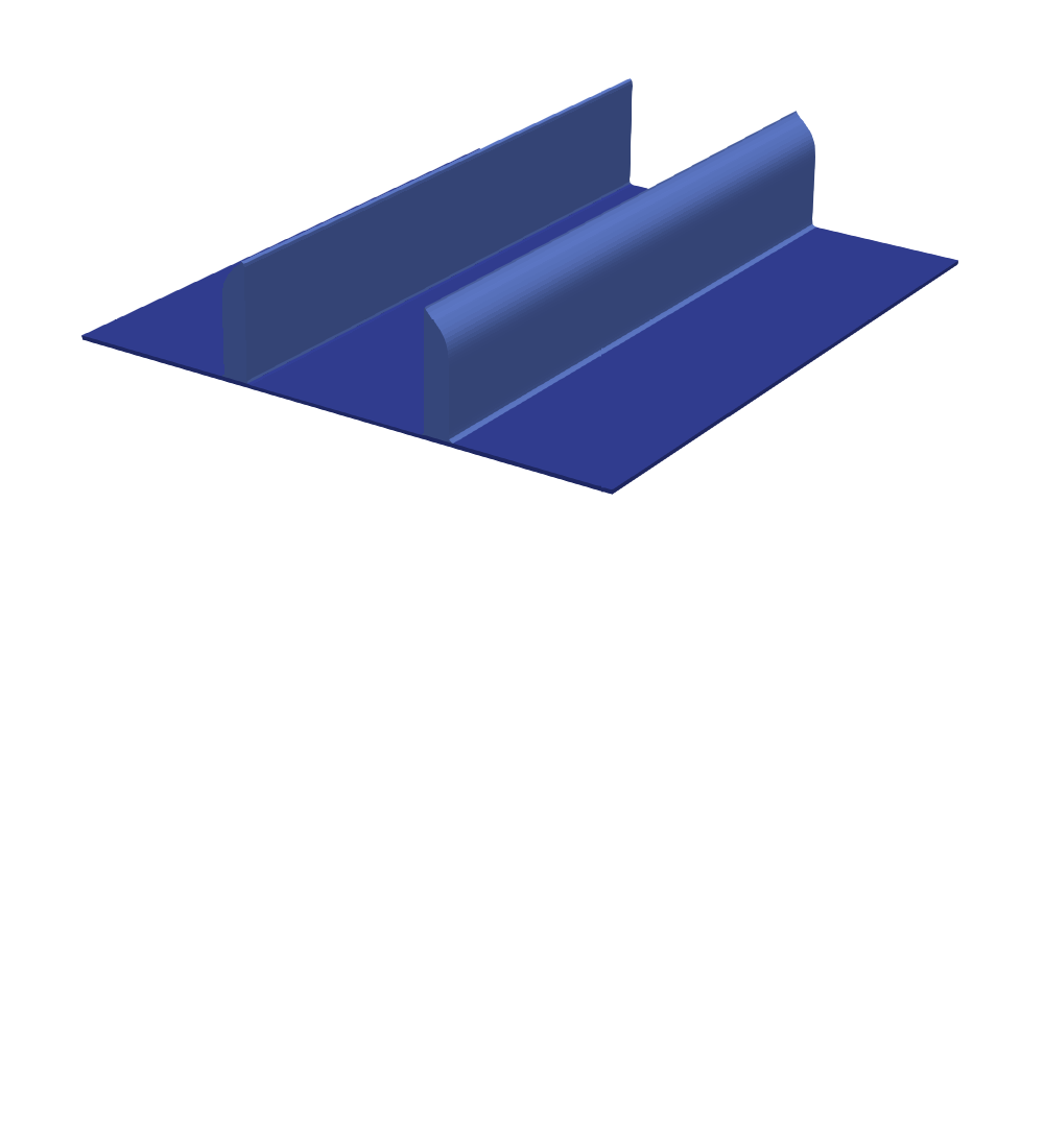
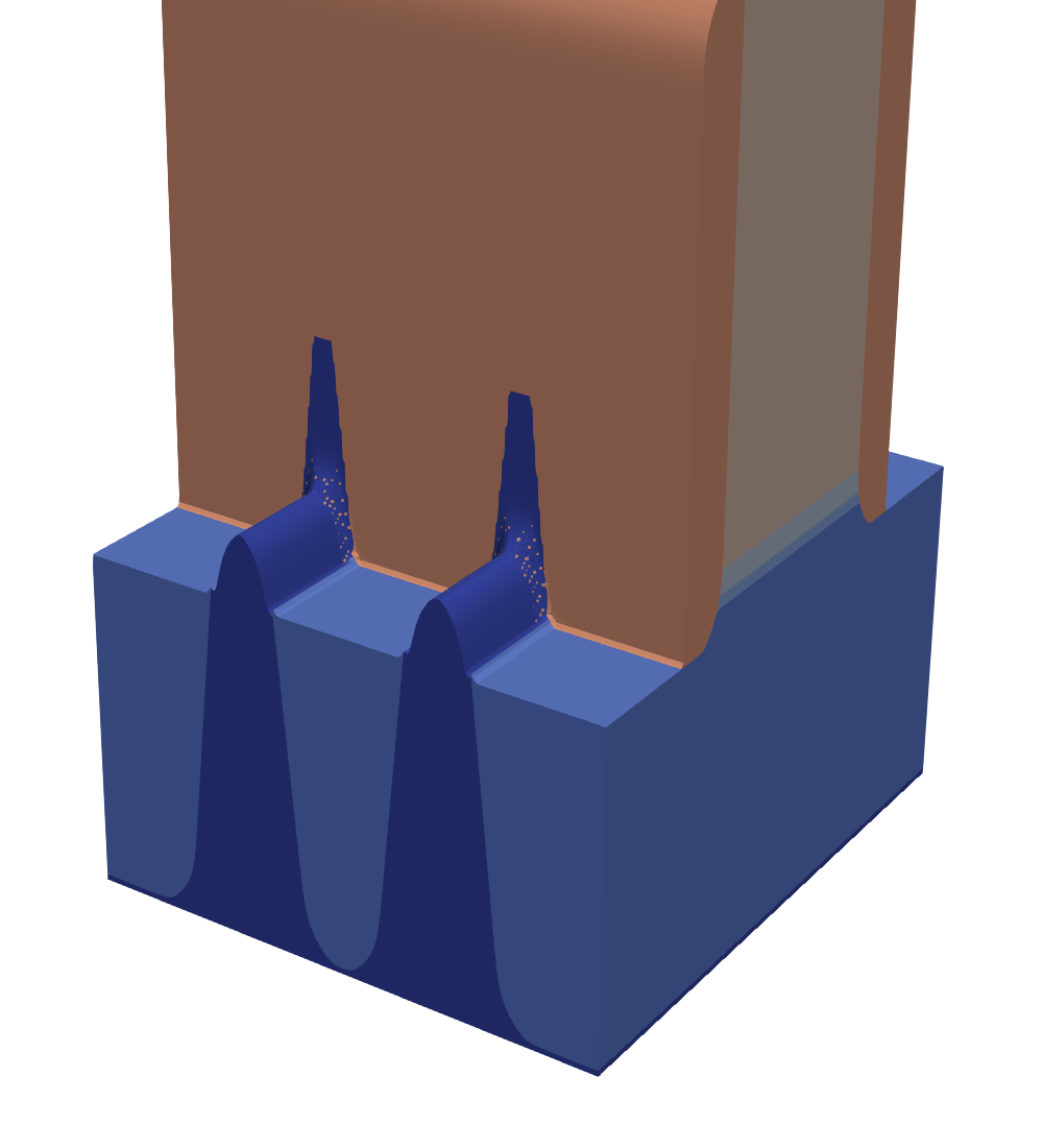
layer is then etched directionally using reactive ion etching (RIE), leaving behind thin pillars of deposited material which are then used as the mask, as shown in Fig. 1.2a. Repeating this
process a second time using the resulting pillars as the initial mask is referred to as quadruple patterning (QP). In order to avoid these complicated multiple patterning techniques, some manufacturers have already implemented
extreme ultra-violet (EUV) photolithography [19].
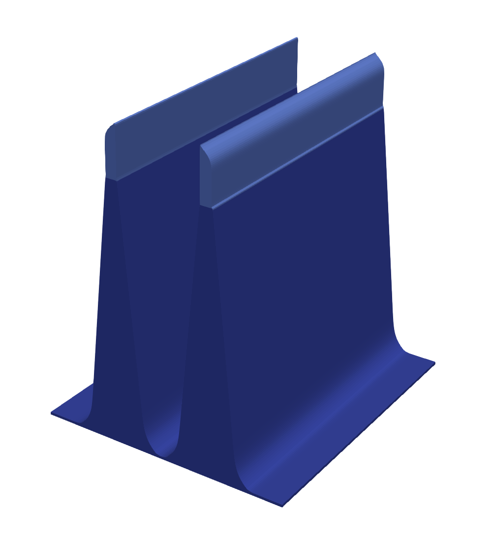
3. Fin Patterning: At this stage, the crystalline silicon substrate is etched, leaving fins below the mask, which will later form the conductive channel of the MOSFET. As indicated in Fig. 1.2b, the etch process is tuned so the fins are positively tapered and thus increase in width towards the bottom.
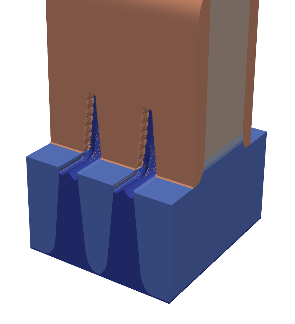
4. Shallow trench isolation (STI): Since each fin may be part of a different transistor, they must be electrically insulated from each other. This is achieved by depositing a dielectric material everywhere. The wafer is then
polished using chemical mechanical planarisation (CMP) to create the flat top surface shown in Fig. 1.2c.
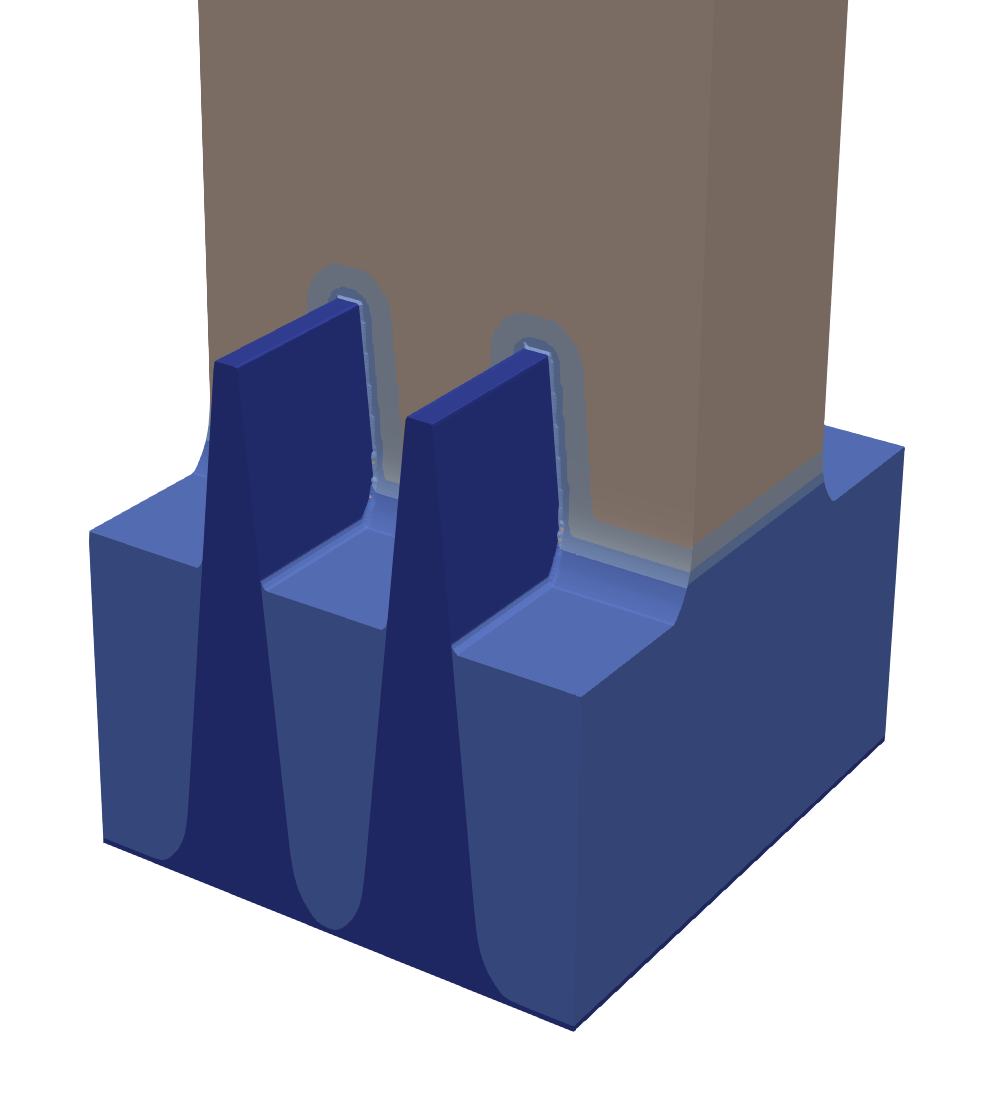
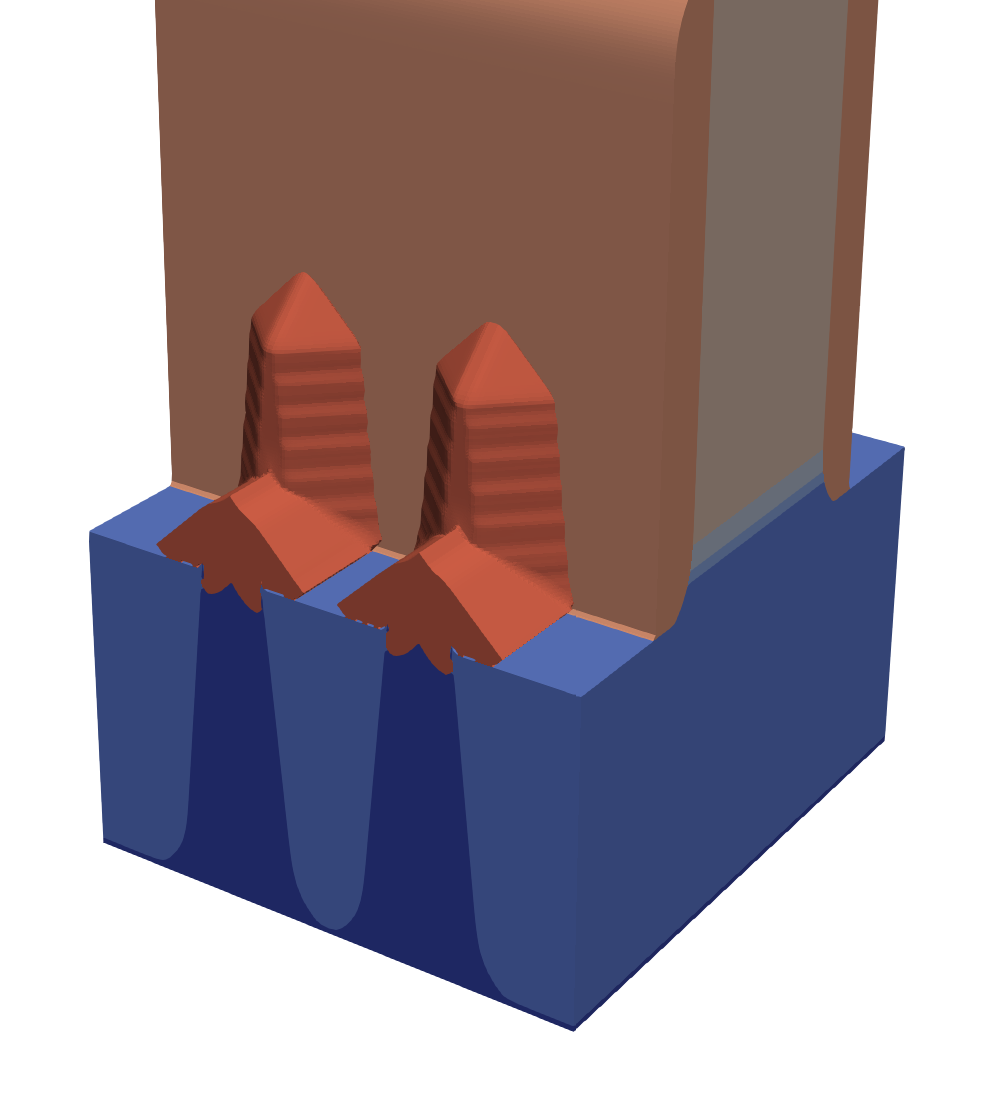
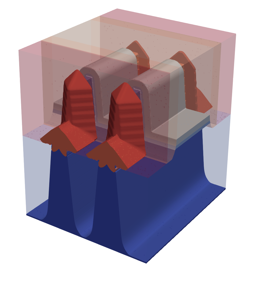
5. Fin Release: Once the surface has been polished, the dielectric can be etched selectively, leaving the crystalline silicon intact. The fins are therefore released again and reach out of the dielectric as shown in Fig. 1.2d, while being isolated from each other to a sufficient depth.
6. Metal Gate Deposition: A high-k metal gate usually consists of a stack of three different materials: A thin layer of a material directly around the fin with a high dielectric constant, often denoted \(\kappa \), hence the
name high-k; Another slightly thicker layer of a metal, referred to as gate metal; And finally a much thicker layer of a gate contact material, usually polycrystalline silicon (poly-Si). These materials are deposited using either CVD
or atomic layer deposition (ALD).
7. Gate Patterning: On top of the gate contact material, another mask is created using photolithography. The gate materials are then etched, one after the other, leaving the gate only covering the centre part of the silicon
fins, as shown in Fig. 1.2e.
8. Gate Spacer: In order to electrically isolate the gate from the source and drain (S/D) regions, a spacer dielectric is deposited isotropically using CVD. Similar to SADP, it is then removed directionally by RIE, leaving the
polymer only on the side of the gate materials. As can be seen in Fig. 1.2f, RIE is not selective and the silicon fins are also eroded during this fabrication step.
9. Fin Recess: The silicon fins are then etched in order to clean them in preparation for the subsequent process, leading to an under-etch of the fins under the dielectric spacer, as shown in Fig. 1.2g.
10. Source and Drain Epitaxy: Now that the surface of the fins has been cleaned, crystalline S/D contacts can be created using epitaxial growth. The rate of this growth varies strongly with the crystal direction resulting in
the characteristic diamond shapes observed in Fig. 1.2h.
11. Interlayer Dielectric: Another layer of dielectric material is deposited to isolate the S/D contacts before the wafer is polished using CMP, resulting in the final MOSFET structure shown in Fig. 1.2i, concluding the FEOL fabrication.
After the FEOL steps are completed, all transistors are connected to form electric circuits during metallisation, which is part of the back-end of line (BEOL). This is performed in several layers, each layer increasing in size,
ultimately providing metal contacts large enough to connect the IC to peripheral components. A single wafer may contain hundreds of chips which are manufactured simultaneously. Since all transistors and interconnects are now
formed, the wafer can be cut into single chips. Each chip is then packaged with connectors suitable for the specific application.
(a) SADP mask on top of silicon substrate.
(b) Silicon fins fabricated using a directional etch into the substrate.
(c) STI deposited and polished in order to isolate individual fins.
(d) Fin release to achieve gate contact with silicon.
(e) Deposition and patterning of the gate stack.
(f) Gate spacer deposition to isolate the gate.
(g) Fin recess.
(h) S/D epitaxy.
(i) Final FinFET structure.
Figure 1.2: FEOL process steps for the fabrication of a 22 nm FinFET.

 [
Home ]
[
Home ]