[
Home ]
[
Home ]
[
Home ]
The precise tuning of process parameters is the most crucial step in the simulation of semiconductor fabrication steps. Since the general setup of any empirical or physical model remains largely as described in Section 3.2, the only differentiating property between models is the set of input parameters. The specific values in each model, such as threshold energy, substrate density, or stoichiometric factors, must therefore be determined experimentally or derived from first principles. This is not only true for sophisticated physical simulations, but also for empirical emulation models, which rely heavily on experimental observations.
In this chapter, several models describing semiconductor fabrication process steps are presented as they have been developed or implemented in the simulation framework developed over the course of this work. Several simulations are based on previously published models and have only been implemented to show the broad capabilities of the simulator, while many other models have been developed over the course of this work and are presented for the first time. The input parameters, as well as their physical source are discussed for each model, highlighting values of highest importance. The results of these models are then analysed and compared to expected analytical results and empirical measurements. Finally, process flows developed during this work for entire devices are presented, which lead to accurate process-aware descriptions of the final geometry. The results of these simulations can be used to extract electrical properties of the device in order to conduct a circuit simulation including variations introduced during the manufacture.
During the course of this work, several models describing single fabrication steps have been developed. In this section, these models are presented and critical features of the resulting geometries discussed. This includes an explanation of the underlying physics as well as particle transport and surface mechanics. The modelling approaches for emulation and simulation are thereafter presented for each model, highlighting their differences and the resulting features observable in the final geometry.
Chemical vapour deposition (CVD) is one of the most commonly used processing steps in the manufacture of semiconductor devices. It is used to deposit a layer of material on top of another substrate and is commonly applied for the deposition of polysilicon [181, 182], silicon dioxide [183], silicon nitride [184] and tungsten [185]. In the simplest case, the feed gas can be simulated by only considering one precursor as the primary source of deposition, as is the case for CVD using silane [186]. In this case, only one particle type needs to be considered in the model and the deposition rate on each surface element is proportional to the incoming flux of this particle type [187]. However, for more complex feed gases or for the combination of several different feed gases into the reactor, more complex behaviours have been observed.
One such example is the deposition of silicon dioxide through tetraethyl orthosilicate (TEOS), where the initial feed gas dissociates into several precursors with highly different properties [188]. It is assumed that TEOS is the predominant precursor, but it only has a very low sticking probability and therefore does not contribute much to the deposition rate, while another molecule which dissociated from TEOS is very reactive and therefore has a high sticking probability. Since this other molecule only makes up a small fraction of all particles in the reactor, it does not completely dominate the deposition rate, rather it ensures subtle non-isotropy on the substrate [188]. Similar models have been previously developed and applied for the CVD of silicon nitride [189] and tungsten [190].
As mentioned in the previous section, in the simplest case, there is only one precursor species responsible for deposition on the substrate. The deposition rate is therefore proportional to the incoming particle flux at each point on the surface. A crude approximation to the flux is achieved by considering the view factor of the source plane for each surface point. If the simplifying assumption of a sticking probability of \(1\) is made, meaning that particles only hit the surface once and then deposit at that location, the deposition rate is directly proportional to the incoming flux. This model will thus only appropriately represent processes with very high sticking coefficients and additional isotropic deposition terms will have to be included to account for lower sticking probabilities. If properties of the initial geometry are known, an analytical expression can be found for the incoming particle flux inside trenches and vias [191]. For an infinite trench, the ideal analytical solution is given by [192]:
\( \seteqsection {5} \)
\begin{equation} F(d) = \frac {1}{2} + \frac {cos(\theta ) - \frac {d}{D}}{2 \sqrt {1 - 2 \frac {d}{D} cos(\theta ) + \left (\frac {d}{D}\right )^2}} \quad , \label {eq::view_factor} \end{equation}
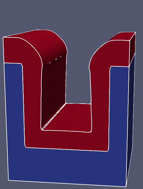
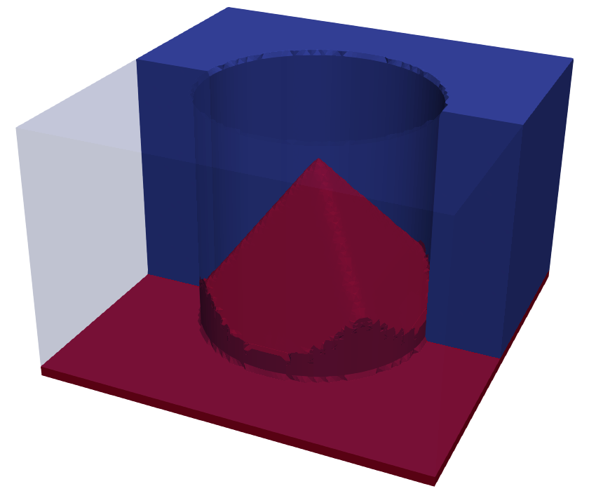
where \(F(d)\) is the view factor of the source plane for a point a distance \(d\) down the trench sidewall which is tapered by the angle \(\theta \). In [106] a pinch-off CVD process for air-gap creation in back-end of line (BEOL) copper lines was emulated using this approach and satisfying results were achieved highly efficiently. Fig. 5.1a shows how each value for the view factor was used as a spherical geometric distribution kernel to achieve the resulting geometry. The generated three-dimensional (3D) geometry shown in Fig. 5.1b is an analytically correct representation of the model described by Eq. (5.1). Despite the model ignoring the build-up of material over time and the resulting change in trench diameter at the top, it produces the expected results exactly and is computationally efficient, due to the geometric advection used to simulate the process.
(a) Schematic showing how the described model creates the resulting geometry (green) using spherical geometric distributions (black circles). The outline of the circles thus creates the final geometry, based on the view factor calculated using Eq. (5.1). Reproduced from [106].

(b) Geometry resulting from the three-dimensional geometric advection model for a pinch-off CVD process for air-gap creation on top of copper lines (orange) depositing a dielectric (blue).
Figure 5.1: Resulting geometry of the geometric advection of a pinch-off CVD process used to generate insulating air-gaps in copper lines through the deposition of a dielectric.
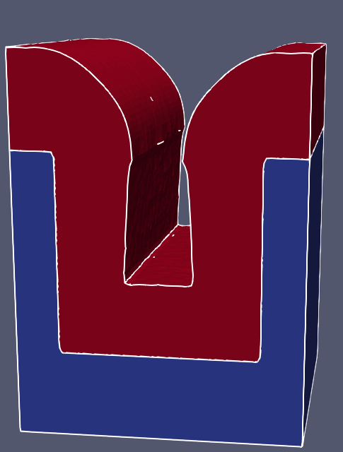
Extending the model from the previous section, intricate physical effects specific to the modelled process can be included in the description. One such effect is the closing of the top of the trench during the process, leading to a smaller and smaller opening though which particles can pass to reach the bottom of the trench. Again, if the initial geometry is known, namely a trench, an analytical model can be used to find the deposition width \(r\) at each point on the initial surface [193]:
\( \seteqsection {5} \) \( \seteqnumber {2} \)
\begin{equation} r(x_s) = \frac {R_{top}}{2} \int _{0}^{t_{total}} dt \int _{\theta _{start}}^{\theta _{end}} \cos (\theta ) d\theta \quad , \label {eq::cvdViewFactor} \end{equation}
where \(\theta \) is the angle from the current initial point on a sidewall, \(R_{top}\) is the deposition thickness at the top surface and \(t_{total}\) is the total time of the processing step. The integrals in this equation can be solved numerically using the forward Euler method which is highly efficient and robust, while providing sufficiently accurate results for this application. The relevant values are depicted in Fig. 5.2a, showing how the closing trench influences the deposition distance at the sidewalls. As the closing rate of the top of the trench can be found analytically, the deposition width at all points of the trench can be also be found analytically, without the need for computationally expensive ray tracing methods. The final 3D geometry is shown in Fig. 5.2b, where the deposited material on top of the trench can be seen to behave differently to the simple model shown in Fig. 5.1b. In this more sophisticated model, the smallest opening of the trench actually occurs high above the initial top surface since the deposited material builds up while growing to the inside. This crucial behaviour could not be modelled using the simple approach discussed in the previous section as deposition was assumed to be constant in time, which is certainly not the case for this type of CVD process. Hence, the time dependence of the deposition and the resulting change in particle traversal through the feature scale region must be taken into account in order to achieve satisfactory results.

(a) Calculation of the deposition thickness \(r\) on the side walls. First, \(R_{top}\) is found using the top visibility, which is then used to find the deposition width \(r\) of points on the side wall.

(b) Slice of the geometry resulting from solving Eq. (5.2) in time using numerical solutions for the time-dependent view factor of a closing trench. The more complex shape of the opening due to the strongly changing view factor is modelled appropriately.
Figure 5.2: Resulting geometry of the geometric advection of a CVD process.
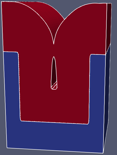
The model presented above requires some knowledge about the initial structure and it can therefore not be applied universally. In order to allow for a full physical description of the process, particle transport and surface chemistry must be modelled. This way, arbitrary initial geometries can be simulated without further considerations, as the model describes the inherent physical nature of the fabrication process without any assumptions about the simulated geometry. A polysilicon deposition process can be modelled straight-forwardly using the modelling framework presented in Section 4.5.1. A two-particle model, similar to the one used in [188], was developed to form an accurate description of the deposition process using TEOS as the feed gas.
From experiments and sophisticated chemical kinetics simulations [183], it has been established that two precursors in the gas phase are responsible for the deposition of polycrystalline silicon (poly-Si) on the substrate. Our physical model involves the simulation of two different types of particles traversing the feature scale region, one representing TEOS with a low sticking probability of around \(10^{-4}\) and one representing the highly reactive precursor triethoxysilane with a sticking probability close to unity \(\approx 1\). This means that there is a strong isotropic growth component through TEOS with a low sticking probability, while anisotropy is generated by the deposition through triethoxysilane. All other modelling parameters are taken from [183], with the simplifying assumption that particles remain on the surface once captured, are not re-emitted, and do not diffuse along the surface. Therefore, the deposition rate is directly proportional to the coverage of the respective particle, similar to the model presented in Eq. (3.17).
The resulting geometries are depicted in Figs. 5.3a to 5.3c and are compared to the experimental data from [188] in Figs. 5.3d to 5.3f. As can be seen clearly, the main features are replicated well for each time step using the sticking probabilities listed above. The overall deposition is strongly dominated by the isotropic growth from TEOS with a very small anisotropy introduced by the deposition of triethoxysilane. Using our model, solving for the deposition rates on top of the trench reveals that the deposition rate of the reactive species contributes roughly 37% of the total deposition rate. Due to the rapidly changing rate for triethoxysilane this results in a clear pinch-off of the trench even for the low aspect ratio used here.
Similarly to the actual process, the model must be tuned to the specific process parameters, such as temperature or pressure. Therefore, any discrepancy with a real process could be incorporated by understanding the physical origin of the behaviour and modelling it in the simulation. Hence, any process can be modelled using this physical approach, with the only disadvantage being long simulation times due to the computational expense of including additional physical effects and the computationally demanding Monte Carlo approach.
Epitaxy is a film growth process during which mono-crystalline layers are formed on top of a crystal substrate [194], which means that the newly grown layer only has one well-defined crystal orientation with respect to the substrate. Epitaxial silicon is usually grown using vapour-phase epitaxy, which is a type of CVD, as the deposited material is introduced to the substrate using precursor gases. In semiconductor fabrication, one of the main applications for epitaxial growth is the deposition of crystalline silicon on top of a wafer substrate of the same material, referred to as homoepitaxy [195].
If a different material to the substrate is grown epitaxially, this process is referred to as heteroepitaxy [196]. This results in a crystal mismatch at the interface between the two different materials, leading to stress inside the material, which may also be temperature dependent [197].
On the atomic scale, epitaxial growth is driven by several physical processes. First, atoms from the gas phase are adsorbed onto the substrate and are loosely bound. These adatoms may now diffuse along the surface, remaining longer at energetically favourable surface sites. Therefore, clusters of adsorbed particles form on the substrate, serving as nucleation sites for other adsorbed particles, as the edges of these clusters form energetically favourable surface sites. As several clusters grow together, they form larger and larger islands, until they coalesce into a film covering the substrate [198]. Due to the fact that clusters of particles form to be energetically compatible with the substrate, they have the same ordering as the crystal they grow on.
Since epitaxial growth is strongly dependent on the atomistic description of the surface, it cannot be described exhaustively using the continuum approach employed in this work. However, the macroscopic effect, namely the growth rates in different crystal directions can be measured experimentally [199] and used for the velocity fields describing the growth of the substrate. Usually, the growth rate is only measured along certain crystal directions, so the growth rates have to be interpolated for all other possible normal directions on the surface. This can be done robustly using the interpolation method presented in [200], which has already been successfully employed in [100, 201]. Assuming that the transport of molecules to the surface does not change drastically across the substrate, the velocity field only depends on the orientation of the surface. Hence, the growth rate can be found given only the crystal orientation of the substrate and the surface normals at each point on the surface.
The exact shape resulting from epitaxial growth depends strongly on the initial geometry and the temporal evolution of the surface. As discussed in [100], whether the fast or slow growth planes will dominate is strongly dependent on the curvature of the initial geometry. For complex shapes of the substrate, the growth might therefore change between fast and slow planes over time and thus a general prediction for which crystal plane will dominate growth is not possible. Due to this temporal dependence of the growth process, it is not possible to formulate a general geometric advection distribution and hence the emulation model has to be carried out using iterative advection. As the growth rates change drastically with the surface normal, the Stencil Local Lax-Friedrichs (SLLF) scheme discussed in Section 2.4.2.4 is used for the iterative advection of the growing substrate.
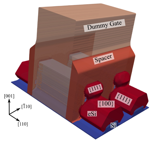
One of the most critical fabrication steps for modern vertical transistors is the epitaxy of the source and drain (S/D) contacts. Using a stacked nanowire field-effect transistor (FET) geometry [202], the model was applied to simulate the formation of the source and drain contacts, resulting in the characteristic shapes produced by fast growing crystal planes shown in Fig. 5.4.
Although continuum models describing epitaxial growth exist [203, 204], they are usually used to examine the fundamental physical processes driving growth rather than the simulation of large structures during fabrication processes. Therefore, the empirical model presented above is used for the description of the surface chemistry, while the necessary particle fluxes are generated using a Monte Carlo (MC) ray tracing approach.
Epitaxial growth of silicon is usually carried out in CVD reactors under specific conditions which allow for crystalline growth. A commonly used precursor is dichlorosilane (Si2H2Cl2) which reacts with the surface to deposit Si forming hydrogen chloride (HCl) as a by-product [205]. The latter can then act as an etching species, slowing the silicon growth rate. However, HCl is required to achieve selectivity of the process, as silicon also deposits on other materials, forming poly-Si films. Due to the lower binding energy of poly-Si to mask materials, compared to the binding energy of crystalline silicon, HCl can remove these unwanted films without etching the crystalline substrate. Therefore, finding the fine balance between the gases which are present in the reactor is critical to achieving selective growth only on the crystalline silicon substrate.
The chemical model was set up as described in [205] and selective epitaxial growth (SEG) on the bottom of a 60 nm wide via was simulated for 140 s. A lack of etchant leads to the unwanted deposition of poly-Si on top of other materials, as shown in Fig. 5.5a. Since no crystalline growth planes are exposed, the deposition of silicon proceeds in an unordered fashion. Only if the correct balance of depositing species and etchant is achieved, does a crystalline silicon film form on top of the substrate and no other materials are affected, as shown in Fig. 5.5b.
Wet etching is one of the corner stones of semiconductor fabrication, especially in the field of microelectromechanical systems (MEMS). Etchants are introduced to the material surface using a liquid solution, which is why this process is called wet etching. Wet etchants usually remove material isotropically, due to the fast and isotropic transport of etchant species to the surface, meaning that every part of the surface is submerged and therefore etched by the solution. For non-crystalline or poly-crystalline substrates, the etching thus proceeds isotropically.
However, crystalline substrates may be etched at very different rates depending on the exposed crystal planes, as certain orientations lead to a more or less favourable bond of surface atoms with the bulk material, meaning that atoms of one crystal plane may be removed more easily than atoms on a different plane [206]. Therefore, crystalline silicon substrates can be etched anisotropically, leading to well defined crystal faces dominating the final geometry.
Similarly to SEG, wet etching can be modelled by considering the etch rates in certain crystal directions and interpolating to all other surface orientations. Additionally, since the process is taking place in a liquid, the etchant transport to the surface is much faster than the etch reaction, meaning the process is only reaction rate limited and there is no need to model particle transport as for SEG. Therefore, an empirical model using empirically determined rates results in a very accurate description and no additional modelling is necessary.
Fig. 5.6 shows the result of a wet etching simulation for a MEMS cantilever, using the same interpolation scheme [200] for the etch rates as used for the modelling of SEG described in Section 5.1.2.
The etch rates for different crystal orientations and temperatures are found in literature [207] and the rates passed to the interpolation scheme simply have to be adapted to the corresponding etch chemistry. Since the etch rates are strongly dependent on the crystal direction, the wafer has to be aligned carefully in order to achieve the desired cantilever structure depicted in Fig. 5.6c. If the wafer is rotated by 45 degrees, an entirely different geometry is produced, as shown in Fig. 5.6d.
In modern semiconductor fabrication, wet etching processes have generally fallen out of favour due to additional cleaning steps which are required to remove residues left on the wafer. Additionally, wet etching processes do not provide enough control over the anisotropy of the etched features for high aspect ratio structures or 3D device geometries [208]. Therefore, most process flows in industrial fabrication of semiconductor devices rely heavily on dry plasma etch processes [209].
Usually, physical etching proceeds through ion-enhanced etching of volatile chemical reactants on the surface of the substrate, as described in Section 3.2.5. However, other mechanisms may also contribute to the etching properties of a process, such as ion energy, ion distribution and the exact surface chemistry. Therefore, in order to develop a reliable plasma etch model, the dominant physical processes have to be identified and their properties carefully tuned to achieve an appropriate description of the underlying physical behaviour.
Silicon is the most important material in semiconductor fabrication, so there is an abundance of etching chemistries developed for the patterning of silicon [210, 211]. Therefore, the chemistries presented in the following section, are mostly concerned with the etching of silicon substrates. Nonetheless, the properties of some of these processes are also discussed for different substrates of interest, such as titanium nitride (TiN) and hafnium dioxide (HfO2) which are commonly encountered in modern FET geometries [212].
Chlorine has been used to etch silicon [213] and several of its compounds, such as silicon dioxide (SiO2) [214], silicon nitride (SiN) [215], as well as other commonly used materials such as TiN, tantalum nitride (TaN) [216] and HfO2 [217].
Plasma etching in molecular or atomic chlorine chemistries proceeds through the adsorption of Cl on the silicon substrate and the formation of SiCl2, which is then desorbed thermally [218] or via ion-enhanced etching of chlorine ions [219]. Several additional gases can be added to achieve different etch properties. The addition of argon [220] or nitrogen [221] as an ion source leads to higher etching yields, due to the increased number of energetic ions assisting in the removal of SiCl2[222].
In the etching of TiN, chlorine may be combined with BCl3 or CHF3 [223], leading to non-volatile BN or TiF4 being deposited on the side walls, respectively. These passivation layers protect the structure from lateral chemical etching through TiClx. Ion-enhanced etching and ion sputtering lead to high etch rates at the bottom of the substrate, leading to anisotropic and highly vertical profiles. These mechanisms for the etching of TiN in a BCl3/Cl/Ar chemistry are depicted in Fig. 5.7.
When etching HfO2, BCl3 plasmas may even be tuned to achieve infinite selectivity to Si, since boron leads to the formation of a thick SiClB layer above the silicon substrate, protecting it from further etching [224]. Thus, BCl3 plasmas are well suited for the removal of the thin HfO2 dielectric layer in modern high-k metal gate FETs [225].
For decades, fluorocarbon (CF) chemistries have been used to etch Si and SiO2 due to the possibility of tuning these chemistries to the etching of different materials with fine control over the selectivity to other materials [226]. In order to adjust the process for specific substrates, a variety of additive gases can be used to change the characteristics of the process [227]. Hence, good etch selectivity can be achieved for certain materials, without infringing on the anisotropic nature of the process [228].
The main etch mechanisms in CF plasmas are chemical etching, ion-enhanced etching and physical sputtering. In the case of silicon, the substrate can be removed chemically by reacting with fluoride to form silicon tetrafluoride (SiF4) which can evaporate back to the gas phase [229], as shown in Fig. 5.8. The rate at which chemical etching proceeds is strongly dependent on the temperature and the amount of carbon on the surface, which may lead to a reduction in etch rates.
Another etch mechanism is the ion-enhanced etching of the substrate, where highly reactive CF+ ions bombard the surface. The substrate is either sputtered by the ion, or the ion reacts with the substrate to form SiF4 which may then evaporate [230]. The temperature should be low enough for SiF4 not to evaporate thermally. Rather, the etch product would be removed by the additional kinetic energy provided by incoming ions. This results in highly anisotropic etching, since substrate can only be removed through energetic ions. However, the ion energy should be as small as possible since ions may otherwise penetrate deep into the substrate, creating impurities. Hence, there is an optimal combination of process temperature and ion energy which leads to highly anisotropic etching with minimal ion-induced damage in the substrate.
Physical sputtering is strongly related to the binding energy of the substrate and appears only above a certain ion energy. The deposition of the passivation layers on the side walls is achieved through the polymerisation of neutral species, such as CF2, which form SiC bonds protecting the substrate. Additionally, deposition may also be driven by direct absorption of energetic ions into the substrate [231].
All of the above discussed etching mechanisms can be described using the general plasma etching model presented in Section 3.2.5. In order to represent this particular chemistry, supplying textbook values for particle and substrate properties is sufficient.
CF plasma chemistries may also be used to etch TiN, although high etch rates can only be achieved at high temperatures, which is why chlorine-based chemistries are commonly used instead [232]. However, the addition of small amounts of CF has been shown to increase the etch rate in chlorine chemistries due to the additional generation of volatile etch reactants in the gas phase [233].
HfO2 which is commonly used as a dielectric, may also be etched in CF plasmas with good selectivity and reasonable etch rates [234]. However, CF chemistries form thick fluorocarbon layers which can be omitted by adding hydrogen as a feed gas [235]. The additional hydrogen will form loosely bound hydrocarbon etch products [236], leading to a significant reduction in carbon contamination. Nonetheless, as HfO2 is often used as an atomically thin dielectric, even small amounts of fluorocarbon residue present a challenge [237], which is why CF chemistries have fallen out of favour when etching HfO2.
A commonly used alternative to CF chemistries is sulphur hexafluoride (SF6) since it allows for finer control over the etch properties through additional gases fed into the reactor while still achieving high etch rates [238]. Without any additional feed gases, pure SF6 dry etching of silicon proceeds isotropically, which can be useful when creating undercuts as it saves the additional cleaning step required after isotropic wet etching [239]. Adding oxygen results in the formation of a thin SiO2 layer being formed on the sidewalls inhibiting lateral etching [240]. The addition of oxygen also leads to higher vertical etch rates, since it binds sulphur, freeing more fluoride which is then available for etching [241]. The oxygen concentration must be tuned carefully, as high concentrations lead to competing surface adsorption with fluoride, forming thick SiO2 protective layers and thus reducing the etch rate [242]. If the oxygen concentration is optimal, only thin SiO2 layers are formed, which are removed on horizontal surfaces through directional energetic ions. Therefore, fluoride atoms can react with the silicon substrate, forming SiF4 which is removed chemically or through ion-enhanced processes [243], similarly to the reactions shown in Fig. 5.8.
The properties of SF6 etching can be tuned through the addition of hydrogen bromide (HBr) and oxygen as feed gases. This leads to the formation of a SiOxBry passivation layer reflecting high energy ions and thus leading to higher vertical etch rates [244]. Therefore, through the introduction of additional feed gases, the behaviour of an etch process might change drastically and a new model describing this behaviour may have to be developed.
Other additional passivating species, such as difluoromethane (CH2F2), have also been successfully applied for the dry etching of silicon [245]. As shown in Fig. 5.9, the build up of the passivation layer on the sidewall is not created through the deposition from the gas phase, but rather through line of sight deposition of sputtered CF etch products obtained from vertical etching [246]. Therefore, the modelling of this process requires an additional ray tracing step, where sputtered etch products are emitted from the collision site of an energetic ion and traced to the sidewall where they might deposit. The thereby created shadowing effects can only be observed with this additional ray tracing step, meaning that this model may incur more computational effort than simpler models. Hence, depending on the modelled process, even the underlying methods used to simulate the model may have to be adjusted.
The described chemistry was implemented using a physical model employing MC ray tracing. The chemical parameters of the involved materials were extracted from [243] and [244]. The model was characterised by simulating the etching of a trench in a silicon substrate for different source fluxes. Fig. 5.10 shows the behaviour of the implemented plasma etch model for these different processing conditions, hinting towards the behaviour of the etch chemistry based on its feed gases. A higher etchant flux thus results in higher etch rates, but a fine balance with the passivating species is required to achieve satisfactory profiles.

Figure 5.10: Two-dimensional trenches formed by etching silicon (pink) with a mask (black). The ion flux was kept constant at 1016cm-2s-1. In a)-c), the trenches were etched for 25 s with a constant etchant flux of 1.3x1016cm-2s-1, while the polymer (blue) concentration was varied: a)5x1015cm-2s-1, b)1016cm-2s-1 and c) 5x1016 cm-2s-1. In d)-f), the polymer flux was constant at 5x1015cm-2s-1 and the etchant flux was changed: d)5x1015cm-2s-1, e)2x1016cm-2s-1 and f) 5x1016 cm-2s-1.
Similarly to fluorocarbon plasmas, SF6 chemistries require high temperatures to etch TiN, although its use as a supplementary feed gas for chlorine chemistries can increase etch rates significantly [233]. Although high etch rates of HfO2 substrates have been achieved in SF6 chemistries, they are limited to low pressures for the appropriate tuning of the selectivity to silicon [234].
HBr chemistries have been in use for a long time to etch silicon for its good selectivity towards SiO2 [130, 247]. Despite the lower silicon etch rate compared to CF and SF6 chemistries, HBr provides excellent selectivity towards other materials, which makes it suitable for the over-etch processing step, used to entirely remove silicon on top of other materials [248]. Ion-enhanced etching typically dominates the removal of the substrate, while the deposition of side wall passivation proceeds mainly chemically [244]. Therefore, simple models can be used to describe the process, as shown in Fig. 5.11. The side walls and substrate are protected by thick SiOxBry layers stopping energetic ions from reaching the material below.
Despite the apparent simplicity of the process, the passivation layer undergoes a change during the process, as bromine is removed from the layer and replaced by oxygen. Therefore, a dense SiO2 layer is generated at passivation layers formed earlier, while an amorphous bromine rich material dominates the passivation layers formed later in the process [249]. This densening of the passivation layers can only be modelled properly using volume information, meaning a pure level set description is not sufficient to capture the process appropriately. It may be approximated by storing the bromine concentration of the material on the surface and reducing it through the thinning of the material, although this may be insufficient for complex geometries. Oftentimes, etching in HBr plasmas is followed by a cleaning step which reduces this layer [250], meaning that it is changed to a dense SiO2 layer everywhere.
A model for this etch chemistry was implemented in ViennaPS using the physical parameters in [249]. Fig. 5.12 shows the profile of a trench etched in a silicon substrate, resulting from HBr etching for different source fluxes of all active species.
Figure 5.12: HBr/O2 etching of Silicon (pink) with a mask (black) for 25 s. The ion flux was kept constant at 1016cm-2s-1. In a)-c), the Si was etched with a constant etchant flux of 1016cm-2s-1, while the polymer (blue) concentration was varied: a)1016cm-2s-1, b)3x1016cm-2s-1 and c) 5x1016 cm-2s-1. In d)-f), the polymer flux was constant at 1016cm-2s-1 and the etchant flux was changed: d)1015cm-2s-1, e)5x1015cm-2s-1 and f) 5x1016 cm-2s-1.
HBr is also well suited for the etching of TiN, achieving satisfactory etch rates [251] and clean final surfaces [237]. However, bromine etches TiN significantly slower than chlorine, although the former can be added in small concentrations to the latter in order to obtain better overall control over etch properties [225].
In order to highlight the simulation capabilities of the presented physical models, a full gate stack etching sequence of a 14 nm gate-first fabrication sequence [208] was simulated using the modelling framework developed during the course of this work. Due to the physical descriptions, not only each process individually, but also the interplay between sequential steps is taken into account. This is especially important when considering different passivation layers building up in each of the etch steps [110].
Poly-Si Main Etch
The first etch step is the poly-Si main etch in a SF6 type plasma chemistry. The model presented in Section 5.1.4.3 was used to simulate this etch step for 60 s with
the model parameters listed in Table 5.1. The geometry of the gate stack after this etch step is shown in Fig. 5.13a. The slanted
side wall stems from the deposition of polymer (blue) layers on the poly-Si (pink), which prevents lateral etching. As expected, the polymer layers are thicker at the top of the structure than at the bottom, since the top side walls
were exposed earlier, leaving more time for the polymer to grow.
Poly-Si Over Etch
After the main etch, a poly-Si over etch step is carried out in a more selective HBrO2 plasma chemistry in order not to damage the TiN underneath. As depicted in Fig. 5.13b, due to the deposition of a several nm thick SiBr-type polymer, the side walls are strongly slanted. Thanks to the selectivity of the etch process, the gate metal underneath the
poly-Si is left intact without damage.
TiN Main and Over Etch
The TiN is subsequently etched in a Cl2CH4 plasma chemistry, which has a lateral to vertical etch ratio of about 0.4, which leads to a visible under etch in the TiN layer. The high lateral etch rate is due
to the small amount of passivating polymer deposited on the sidewalls, as can be seen in Fig. 5.13c. This wears down the previously deposited passivation layers, which now play an
important role in protecting the poly-Si from the etchant.
In order not to damage the thin high-k dielectric HfO2 layer underneath the TiN, a more selective etch process is used for the over etch step. The etching in a Cl2/N2 chemistry proceeds highly isotropically and appropriately cleans the HfO2 surface for the last etch step, as shown in Fig. 5.13c.
HfO2 Etch
The HfO2 layer which is only a few nanometres thick, is then etched in a BCl3/Cl2 plasma. This etch chemistry also proceeds highly isotropically and has a near-infinite selectivity against the
SiO2 substrate underneath the gate dielectric [224]. The final structure after this etch step is visualised in Fig. 5.13d, which highlights the importance of the previously
deposited passivation layers to protect the masked gate stack from etching in the subsequent, more isotropic etch steps.
| Process Step | Model | Ion Flux | Etchant Flux | Polymer Flux |
| Poly-Si ME | SF6/CH2F2 | 1.5 · 1015 | 1.3 · 1016 | 4.5 · 1015 |
| Poly-Si OE | HBr/O2 | 1.0 · 1016 | 1.0 · 1016 | 2.0 · 1016 |
| TiN ME | Cl2CH4 | 1.0 · 1015 | 5.0 · 1015 | 2.8 · 1016 |
| TiN OE | Cl2/N2 | - | 1.0 · 1017 | 1.0 · 1016 |
| HfO2 Etch | BCl3/Cl2 | - | 1.1 · 1016 | 6.2 · 1015 |
Table 5.1: Model parameters of the physical models used to simulate the gate stack etching sequence with fluxes given in units of /(cm2 s). Main etch and over etch chemistries are indicated as ME and OE, respectively. All models were simulated using a pressure of 1.35 Pa with a bias voltage of 60 V for the plasma etch steps.
Figure 5.13: Gate stack geometry after important patterning steps, highlighting the importance of passivation layers throughout the process. The thick, protective layers formed during the poly-Si etch steps protect the material throughout the process.
The cyclic Bosch Process [252] was developed in 1994 for generating high aspect-ratio structures in the field of MEMS [253, 254]. Since then, this fabrication technique has become important for numerous other applications, such as 3D integration [255, 256], high bandwidth memory [257, 258] and even on-chip wireless communication [259].
This process is a type of deep reactive ion etching (DRIE), where sidewall passivation and etching do not proceed simultaneously but are separated into individual steps carried out sequentially. By repeating these sequential process steps many times, aspect ratios far higher than those achievable using conventional plasma etching approaches have been achieved [260]. The original approach will be discussed in the following section, followed by further developments through the introduction of additional processing steps.
This sequence of process steps was used when the Bosch Process was first introduced. It consists of a deposition step followed by a plasma etching step, which is why this approach is also referred to as the deposit-etch-multiple-times (DEM) sequence. Since the etch step is not perfectly anisotropic, a scallop is formed during each cycle of the process, as depicted in Fig. 5.14.
However, robust sidewall passivation and very straight profiles can be achieved reliably, reducing sidewall tapering significantly compared to other plasma etching processes. However, when the etched structures reach aspect ratios higher than 50, reactive ion etching (RIE) lag is observed [261, 262]. Due to a smaller and smaller number of etchant particles and ions reaching the bottom of the structure, the etch rate decreases significantly until etching is perfectly balanced with the deposition step at the bottom of the generated structure. This effect can be reduced by increasing etch times for later cycles, but due to the prolonged etch step, the mask or top of the structures can be worn away quickly [263].
Due to the problems encountered during the etch step of the DEM sequence for high aspect ratios, this step can be split once again [264]. In order to remove the protective layer at the bottom of the structure, a low pressure etching process is conducted at high plasma bias, resulting in highly anisotropic etching [260]. After this step, the exposed substrate is etched isotropically at low bias, as shown in Fig. 5.15. Due to the additional passivation removal step, this procedure is referred to as the deposit-remove-etch-multiple-times (DREM) sequence.
Due to the separation of the etch step, a shorter time under high bias is required, leading to higher mask selectivity [265]. For high aspect ratios, RIE lag can thus be countered by only increasing the isotropic etch time, which leads to uniform scallop sizes down the feature without damaging the mask [266].
However, if the deposition of the protective layer and its removal are not perfectly balanced, more polymer may be deposited on the top opening than necessary. Therefore, each cycle increases the thickness of the protective layer at the top, effectively closing off the opening. This increases shadowing and thereby reduces the number of high energy ions reaching the bottom of the structure to remove the protective layer [265], leading to a smaller hole in the deposited material at the bottom of the feature. Due to the time ramping of the isotropic etch step, the scallop size does not change drastically, but the smaller hole sizes are copied down, resulting in tapered side walls.
As described in the previous section, the pile-up of polymer can only be avoided by carefully tuning the interplay of the deposition and removal of the protective layer. However, tuning these steps is time consuming and may require frequent calibration.
The buildup of polymer at the top opening may also be avoided by introducing an additional ashing step [267], which selectively removes the polymer, leading to a clean surface [268]. This is performed with the so-called deposit-remove-etch-ash-multiple-times (DREAM) sequence which is shown in Fig. 5.16. This method prevents the closing of the hole opening and the subsequent tapering without the need for frequent and precise tuning.
Due to the complex final structure generated by the DRIE process, two separate geometric advection steps are necessary to create it:
1. Smooth Profile: The profile describing the outline of the high aspect-ratio feature is generated.
2. Scallops: The scallops produced by the cyclic nature of the process are formed, starting with the smooth profile.
Since the exact physical nature of how the structure was generated is not important in process emulations, these two steps suffice to generate the final structure. This is independent of the number of cycles that would be needed in the actual fabrication of the structure and is thus highly efficient.
Smooth Profile
Since the final profile will be highly directional, a rectangular geometric advection distribution is used to generate the smooth outline. The edge length of this distribution will be \(L\), which is given by the number of cycles
\(N_c\) times the etch depth per cycle \(d_c\)
\( \seteqsection {5} \) \( \seteqnumber {3} \)
\begin{equation} L = N_c d_c \quad . \end{equation}
As discussed in the previous sections, decreasing etch rates may also lead to tapered side walls. Therefore, tapering is modelled by reducing the total etch depth \(L\) according to the lateral distance to the mask. During DRIE, the side walls are usually tapered inwards, meaning the feature becomes smaller with increased etch depth. Therefore, the coordinate dependent etch depth \(L(\vec {x})\) is smallest at the sidewall and increases with the lateral distance to masked regions.
Scallops
The smooth profile generated in the first step is the starting geometry for scallop creation. Since the scallops are produced by the isotropic etching of the substrate, they can be emulated using spherical geometric advection
distributions. These distributions should only be placed at points, where the substrate was initially available for isotropic etching. Therefore, the radii of all geometric distributions are set to zero, except at the heights where
scallops would be formed by the process. Therefore, ignoring tapering, the \(n\)th scallop is formed at a height \(z_n\) given by
\( \seteqsection {5} \) \( \seteqnumber {4} \)
\begin{equation} z_n = d_c \left (n + \frac {1}{2}\right ) \quad \text {for} \; n \in \mathbb {Z} \quad . \end{equation}
The diameter of the spherical distributions centred at \(z_n\) is given by the isotropic etch distance per cycle \(d_{iso}\) which is closely related to the etch depth per cycle \(d_c\). If the physical phenomena driving the etching are dominated by free molecular transport, \(d_c\) and \(d_{iso}\) are equal. However, if the etch process is mostly diffusion-limited, then \(d_{iso}\) is larger than \(d_c\). Therefore, it is useful to express \(d_{iso}\) as a multiple of \(d_c\):
\( \seteqsection {5} \) \( \seteqnumber {5} \)
\begin{equation} d_{iso} = f_t d_c \quad , \end{equation}
where \(1 \leq f_t \leq 2\). The difference between the two transport phenomena is shown in Fig. 5.17 for the extreme cases of perfect free molecular transport when \(f=1\) and perfect diffusion-limited transport when \(f_t=2\) in Section ?? and Section ??, respectively. Usually, a combination of both transport phenomena is observed and the common value of \(f_t \approx 1.5\) for modern plasma etching processes [211, 267] is also shown in Section ??.
The spherical distributions discussed so far imply that etching is perfectly isotropic, meaning that the lateral and vertical etch rate are equal. However, this may not always be the case and, especially in modern SF6 plasma chemistries, lateral etching is usually slower than vertical etching. In order to capture these differing etch distances, it is useful to express the lateral etch rate \(R_l\) as a fraction of the vertical etch rate \(R_v\)
\( \seteqsection {5} \) \( \seteqnumber {6} \)
\begin{equation} R_l = f_l R_v \quad , \end{equation}
where it is assumed here that \(0 \leq f_l \leq 1\) holds.
The geometric advection distribution, taking the anisotropic rates into account, resembles a spherical cap shape similar to a convex lens, as shown in Fig. 5.18, and will be referred to as lens distribution in the following. Graphically, this distribution is created by removing the centre section of a unit sphere in all lateral directions and moving the slices back to the origin. The centre section ranges from \(-1(1-f_l)\) to \((1-f_l)\) in the lateral dimensions, as shown in Fig. 5.18a. The outer parts of the sphere are then moved back to the origin and scaled by \(r_{lens}\) to achieve the original etch depth of \(d_{iso}\). The correct scaling is achieved by defining \(r_{lens}\) as
\( \seteqsection {5} \) \( \seteqnumber {7} \)
\begin{equation} r_{lens} = \frac {d_{iso}}{2} \begin {cases} 1 & \text {if} \quad f_l \geq 1\\ \left (1 - f_l^2\right )^{-1/2} & \text {if} \quad 0 \leq f_l < 1\\ \text {undefined} & \text {if} \quad f_l < 0 \end {cases} \quad . \end{equation}
The lens distribution is then defined by adjusting the definition for the spherical distribution and is given by
\( \seteqsection {5} \) \( \seteqnumber {8} \)
\begin{equation} \phi _{lens}(\vec {v}, f_l) = \frac {| \vec {v} + (1 - f_l) r_{lens} {\overrightarrow {\text {sgn}}}(\vec {v}_{D})| - r_{lens}}{\Delta x} \quad , \end{equation}
where \(\vec {v}_D\) consists only of the lateral dimensions of the vector \(\vec {v}\), meaning \(\vec {v}_2 = (v_x, 0)\) and \(\vec {v}_3 = (v_x, v_y, 0)\) for two and three dimensions, respectively. \(\overrightarrow {\text {sgn}}(\vec {v})\) is the sign function of the vector \(\vec {v}\). The additional term \((1 - f_l) r_{lens} {\overrightarrow {\text {sgn}}}(\vec {v}_{D})\) as compared to Eq. (2.65) essentially shifts the distance vector \(\vec {v}\) outside of the spherical distribution, creating the lens distribution shown in Fig. 5.18a.
This distribution can fully describe the scallops created by an anisotropic etch step, as those generated in modern Bosch process cycles. An example for such scallops using typical values is shown in Fig. 5.18b, showing a clear difference to the scallops generated by the spherical distributions shown in Fig. 5.17.
Figure 5.18: (a) Starting from a spherical distribution, a lens distribution can be created by removing the centre part. The vector \(\vec {v}\) is translated to the remaining parts. (b) Using this lens distribution, a difference in vertical and lateral etch rate can be modeled for \(f_t = 1.5\) and \(f_l=0.5\). CC BY 4.0 [269]
DEM Sequence
In high aspect ratio structures this sequence suffers from RIE lag, which means that the etch rate decreases with increasing aspect ratio [270], due to the depletion of etchant particles at the feature bottom [271].
Therefore, the feature will become smaller with increasing depth due to the positively tapered side walls. The decrease in etchant particle flux down the feature depends on the exact geometry and particle transport in the feature scale region. The simplest approximation is to assume that the etchant flux decreases linearly after a certain depth \(L_t\). Each cycle performed below this depth will then be affected by the reduced etch rate. Given the total number of cycles \(N_c\) and the depth at which tapering starts, the number of tapered cycles is given by
\( \seteqsection {5} \) \( \seteqnumber {9} \)
\begin{equation} N_t = N_c - \frac {L_t}{d_c} = N_c - N_s \quad , \end{equation}
where \(N_s\) is the number of cycles unaffected by the tapering.
The depth of the rectangular distributions \(L(\vec {x})\) used to generate the smooth profile is then given by
\( \seteqsection {5} \) \( \seteqnumber {10} \)
\begin{equation} L({\vec {x}}) = \min \left (L_{t} + \frac {| \vec {x} - \vec {m} |}{w_{t}} (L_0 - L_{t}) , L_b\right ) \quad , \label {eq::DEMSmooth} \end{equation}
where \(w_t\) is the tapering width, which is the lateral distance between the tapered side wall and a straight side wall at the bottom of the structure. \(L_0\) is the depth at which the etch rate would balance the deposition rate, so it represents the maximum depth achievable with the process, \(\vec {m}\) is the laterally nearest point on the mask surface to \(\vec {x}\) and \(L_b\) is the bottom of the structure after the process given by
\( \seteqsection {5} \) \( \seteqnumber {11} \)
\begin{equation} L_b = L_t + \bar {z}_{N_t}(d_c, D) \quad , \end{equation}
where \(D\) is the depth along which the etch depth per cycle decreases from \(d_c\) to zero. This depth is given in Appendix B.1 and is used to find the total depth of all tapered cycles \(\bar {z}_{N_t}(d_c, D)\). This depth depends only on the number of tapered cycles and the ratio of the etch depth of the final cycle and the initial etch depth per cycle \(d_c\), denoted as \(r_e\):
\( \seteqsection {5} \) \( \seteqnumber {12} \)
\begin{equation} r_e = \frac {d_{N_t}}{d_1} = 1 - \frac {w_t}{w_{tot}} \quad , \end{equation}
where \(w_{tot}\) is the tapering width at depth \(L_0\), which are both properties of the specific etch process and must therefore be tuned to the precise chemistry used [272]. If several features of different sizes should be modelled simultaneously, \(w_{tot}\) and \(L_t\) may also have to be adjusted depending on the size of each feature, in order to include effects such as aspect ratio dependent etching (ARDE) [273].
Once the straight profile has been obtained for the DEM sequence, the radius of all scallops must be found. They will be constant until tapering starts at depth \(L_t\). They will then decrease during each cycle, with the \(n\)th radius given by
\( \seteqsection {5} \) \( \seteqnumber {13} \)
\begin{equation} d_n = d_{iso} \begin {cases} 1 & \text {if} \quad n \leq N_s\\ 1 - \left (\bar {z}_{N_t}(d_c, D) - L_t\right ) / D & \text {if} \quad n > N_s \end {cases} \quad , \end{equation}
with the lens distributions describing the \(n\)th scallop centred at the height
\( \seteqsection {5} \) \( \seteqnumber {14} \)
\begin{equation} z_n = \begin {cases} d_c n & \text {if} \quad n \leq N_s\\ d_c N_s + \bar {z}_{n}(d_c, D) & \text {if} \quad n > N_s \end {cases} \quad . \end{equation}
The above model for the DEM sequence was used to emulate a structure from [265] and the resulting geometry was compared to experimental data. As shown in Fig. 5.19, the decreasing scallop size observed in the experiment is matched well by the simple approximation of a linear decrease in etchant flux down the feature. Despite the resolution of the level set (LS) being barely sufficient to properly represent the smallest scallops, the model can produce an accurate description of the final structure without introducing numerical artefacts, as is often the case when using iterative advection schemes [274]. The model parameters used to perform the emulation are listed in Table 5.2 and hence describe the modelled chemistry and can be applied to different geometries, providing reliable results for any geometry or number of cycles.

Figure 5.19: (a) DEM process without tapering, but a decrease in scallop sizes down the feature. (b) Emulation of the same process with \(N_c=50\). CC BY 4.0 [269]
DREM Sequence
The tapering of the smooth profile for the DREM sequence can be modelled similarly to the DEM sequence through the use of thin vertical box distributions changing in depth depending on their proximity to the mask. Therefore,
the vertical distribution can also be described by Eq. (5.10). However, due to the differing physical mechanisms leading to the tapering, the definitions of
\(L_0\) and \(L_b\) differ from those of the DEM sequence. In the DREM sequence, the scallops are constant in size down the feature and therefore the bottom of the trench \(L_b\) is simply
\( \seteqsection {5} \) \( \seteqnumber {15} \)
\begin{equation} L_b = L_t + d_c N_t = d_c N_c \quad . \end{equation}
The maximal depth achievable with the modelled process \(L_0\) is then given by
\( \seteqsection {5} \) \( \seteqnumber {16} \)
\begin{equation} L_0 = L_t + \frac {d_c N_t}{1 - r_e} = L_t + \frac {d_c N_t}{w_t / w_{tot}} \quad , \end{equation}
which means that \(w_t\) describes how the closing of the top of the feature affects the removal of the protective layer at the bottom of the trench. If there is no tapering, \(w_t = 0\) and there is no effect on the trench. However, if \(w_t \geq w_{tot}\), the top of the feature is pinched off entirely and therefore the tapered side walls meet at the bottom of the feature. Therefore, etching stops since no etching species can reach the bottom at this stage. Due to the segregation of the removal of passivation and the etching of the substrate, time ramping can be used to ensure scallops which are constant in size, as described in Section 5.1.6.2. Therefore, no additional considerations are necessary to describe the scallops down the feature as long as the time ramping is tuned correctly. If the time ramping, however, is not conducted adequately, then the DEM sequence model can be used to describe the resulting geometry.
A well tuned DREM process was simulated using the above model to emulate the sausage-chain-like pillars presented in [265]. Since pillars, rather than vias, are etched, particle transport to the bottom of the feature is not of great concern and it can be assumed that the sequence is tuned well. The structure is generated using 8 cycles of a DREM sequence followed by an isotropic etch step creating an under etch resulting in a large scallop at the end. In the original experiment, these 8 cycles plus an isotropic etch are repeated 8 times to generate tall pillars resembling sausage chains in appearance. Using the geometric DREM model, the 3D structure shown in Fig. 5.20 was created using the model parameters listed in Table 5.3. The final structure consists of 72 individual pillars represented using 3,827,322 LS values and shows good agreement with the structure generated in [265] shown on the right in Fig. 5.20.
Due to the efficient algorithm employed for the emulation of the geometry, even large geometries can be created quickly, including process-specific effects which may strongly influence the final structure and lead to significant changes in the electrical characteristics of the structure. Therefore, even large and complex structures can be generated efficiently, allowing for the process-aware generation of entire devices, such as MEMS actuator [275] or photonic crystals [276].
| \(L_t\)[µm] | \(d_c\)[µm] | \(f_t\) | \(f_l\) | \(r_e\) | |
| - | -0.25 | 1.20 | 0.50 | 1.00 | |
Table 5.3: Model parameters for the DREM model used to generate the sausage-chain-like geometry in Fig. 5.20.

Figure 5.20: (a) Emulation of sausage-chain like structures using several DREM sequences, as well as longer intermittent isotropic etch steps. (b) SEM image of the sausage-chain pillars generated by the DREM process. The emulation was performed using 32 threads and took 14 minutes and 52 seconds to execute. 80 cycles of the DREM model were performed without tapering using the fitting parameters given in Table 5.3. In order to generate the isotropic etch sections, every 10th scallop’s isotropic etch depth was increased to \(d_{iso}=-1.0\). CC BY 4.0 [269]
DREAM Sequence
The distributions required to describe the DREAM sequence are the same as those used in the DREM sequence. Since the additional ash step prevents the closing of the top of the feature, only this process step influences the
tapering width [266]. If it is not effective, the pile up of material on top leads to the time ramping failing due to the smaller top opening. Therefore, scallop sizes cannot be kept constant and RIE lag, similar to that of the DEM
sequence, is observed. Therefore, in order to describe the DREAM sequence, the model parameters can be adjusted according to the applied ash time.
In the simplest case, only the ratio between the initial and the final scallop \(r_e\) is adjusted according to the ash time \(t_a\). Using a simple model based on Knudsen diffusion down the feature to describe the changing properties of the process with changing ash time (see Appendix B.2), the scallop ratio is given by
\( \seteqsection {5} \) \( \seteqnumber {17} \)
\begin{equation} r_e(t_a) = p_0 - \frac {p_1}{p_2 + t_a} \quad , \label {eq::DREAM_model} \end{equation}
where \(p0\), \(p1\) and \(p2\) are fitting parameters. Using experimental data from [267] and [266], \(r_e\) was calibrated to the ash time per cycle assuming constant \(N_c\) and \(L_t\), resulting in fitting values of \(p_0=1.17\), \(p_1=0.59\), \(p_2=-0.44\) (see Appendix B.2 for details). Since \(0 \leq r_e \leq 1\), ashing will only influence the result if it lasts longer than the minimal ash time \(t_0 = p_1/p_0 - p_2 = \SI {0.94}{\second }\) and no additional effect is observed for ash times longer than \(t_m = p_1/(p_0 - 1) - p_2 = \SI {3.91}{\second }\).
Therefore, if the ash time approaches zero, the DEM model is recovered, while for the maximum ash time, the result is equivalent to that of a perfectly tuned DREM model. The model described above was used to emulate a series of high aspect-ratio vias using the model parameters shown in Table 5.4. As can be seen in Fig. 5.21, the results match the experimental data quite well over the entire range of ashing times.
| \(L_t\)[µm] | \(d_c\)[µm] | \(f_t\) | \(f_l\) | \(r_e\) | |
| -24.96 | -0.37 | 1.20 | 0.50 | \(r_e(t_a)\) (see Eq. (5.17)) | |
Table 5.4: Model parameters for the DREAM sequence used for a series of via etch emulations with changing ashing time.
Figure 5.21: DREAM Sequence simulations for \(N_c=100\) with different ash step times compared to experimental data. Only the ash time was varied as input for the DREAM model, while all other parameters were fixed with values provided in Table 5.4. CC BY 4.0 [269]
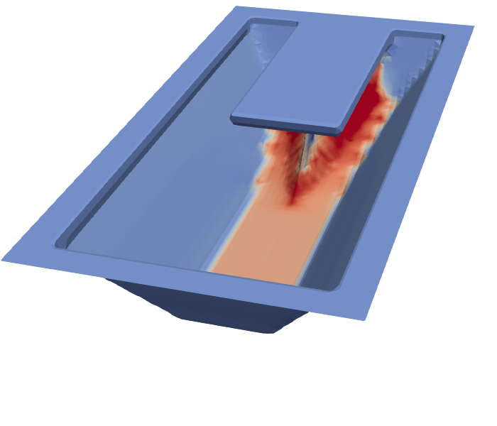
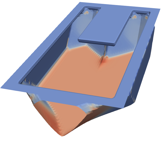
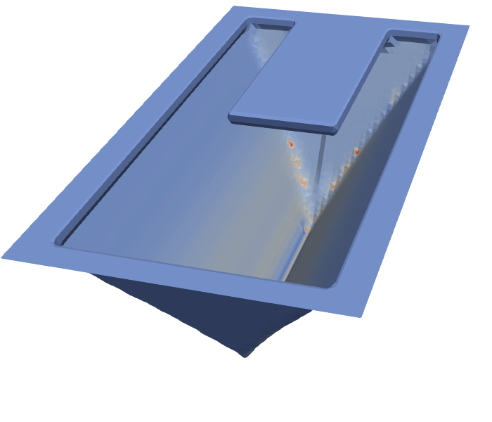
In order to predict transport phenomena or to evaluate new chemistries whose effect on the structure is not known, a physical model is required. Emulation cannot provide any features due to wrong process parameters, such as too high etchant fluxes during a process. However, these properties are especially important when considering many cycles of a Bosch Process, where fluxes may change drastically down a trench geometry. In order to display these effects, a physical model for the clear-oxidise-remove-etch (CORE) sequence presented in [267] was implemented.
First, the surface is cleared from any contamination such as left over polymer in the Clear step. This is conducted similarly to the ash step of the DREAM sequence, in a dry O2 chemistry without any plasma bias. In this physical model, this process step is simulated using MC ray tracing of a single particle species which isotropically and selectively removes materials other than silicon. Due to its high selectivity, it can be applied for longer times without damaging the underlying substrate.
Secondly, the surface is oxidised for a few seconds at higher O2 pressures. This step was modelled similarly to the Clear step, but due to the higher chamber pressure, more oxygen radicals actually hit the surface, which is why this process step was simulated with a much higher source flux. When oxygen radicals contact the surface, they form thin SiO2 layers, protecting the substrate in the subsequent etch step. Since these layers are very thin and only small amounts of the substrate are lost to the oxidation, this step was modelled as isotropic deposition with input parameters as shown in Table 5.5. This is more efficient than physically modelling oxidation which requires both the substrate and the oxide surface to be advanced depending on their width.
Next, the remove step is carried out in a SF6 plasma at plasma bias and low pressure to ensure that ions gain enough energy without colliding with other species in the reactor scale. This step is modelled using the SF6 plasma model described in Section 5.1.4.3. Since there is no polymer flux, no sidewall deposition is observed and the protective SiO2 layers are removed highly directionally. This step is modelled using different ion and neutral etching species, leading to ion-enhanced etching of the polymer and the substrate once it is exposed.
In the final etch step, the SF6 flow rate is increased and there is no plasma bias anymore, which means that etching proceeds isotropically. The etch time must be set carefully because it sets the scallop size and may lead to defects in the final structure if it is too long. Such damage can be seen in Fig. 5.22, where the passivation was not thick enough to sustain prolonged etching times. This results in additional under etches which create unwanted holes in the side walls. Furthermore, the time ramping discussed in Section 5.1.6.2 must be applied in order to ensure uniform scallop sizes for later etch steps.
Much like the real process, physical modelling is driven by underlying descriptions of the interacting molecules and the surface. Therefore, careful tuning and fitting of process parameters is also necessary in every physical model. Due to the modelling of the underlying physics of the process steps, the behaviour of etch chemistries or more complex etch cycles, such as the CORE sequence, can be evaluated. Hence, physical models can be used to test the applicability of new chemistries or processing techniques.
However, due to the more intense fitting effort compared to empirical emulation models, physical models are not well suited for quick and efficient structure generation. In this case, it is more appropriate to include required properties in geometric models and apply them to structures of interest.