[
Home ]
[
Home ]
[
Home ]
Using the models developed during the course of this work, as presented in the previous section, a full process flow for the manufacture of a semiconductor device can be simulated or emulated. When the models are applied correctly, specific process-induced effects on the final device can be observed and can aid in the understanding of the effect of processes on specific properties of a device. Especially effects which stem predominantly from the combination of fabrication steps can be modelled this way, giving insights into the underlying physical effects which might lead to unexpected features of the final device. For example, a cleaning step may be necessary between two sequential fabrication steps due to the first process contaminating the substrate, which negatively impacts the successful execution of subsequent processing steps.
In this section, several full process flows used to generate entire devices will be presented. The exact combination of processing steps used to create the devices are taken from literature, using commonly observed values for unpublished process characteristics. Therefore, the models presented in this section should not be seen as exact replications of certain device processing flows. They rather present proofs of concept for the simulation of large structures using a combination of interdependent physical and empirical process models for the process-aware generation of full device geometries. In this way, dominant physical mechanisms can be identified and investigated in detail to find optimal processing conditions for the generation of complex structures.
The process flow for the production of the 22 nm transistor employs self-aligned double patterning (SADP) for the definition of the fins on a bulk silicon substrate [277]. The high-k metal gate (HKMG) [278] is manufactured using the replacement metal gate (RMG) process [279], where the high-k material is deposited before the poly-Si dummy gate. During dummy gate removal through selective etching, this thin dielectric layer is left intact and the S/D regions are protected by the interlayer dielectric (ILD). In the final front-end of line (FEOL) processing step, the metal and gate contact materials are then deposited on top of the existing layer.
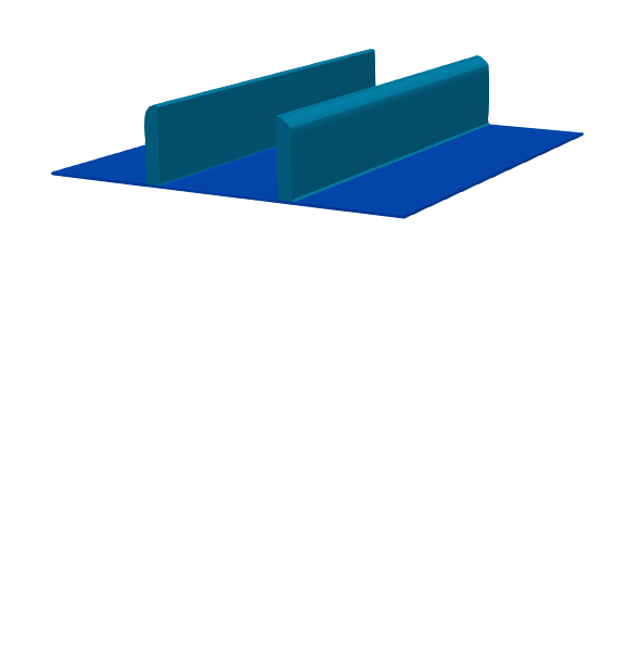
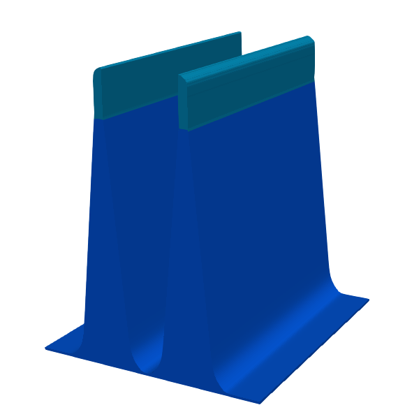
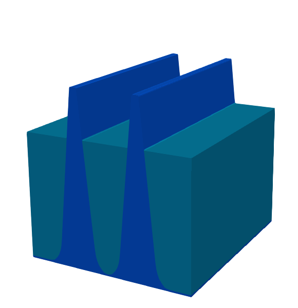
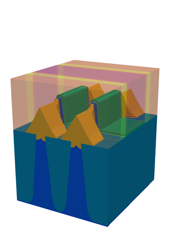
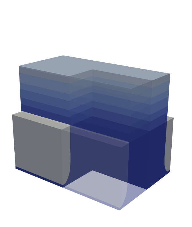
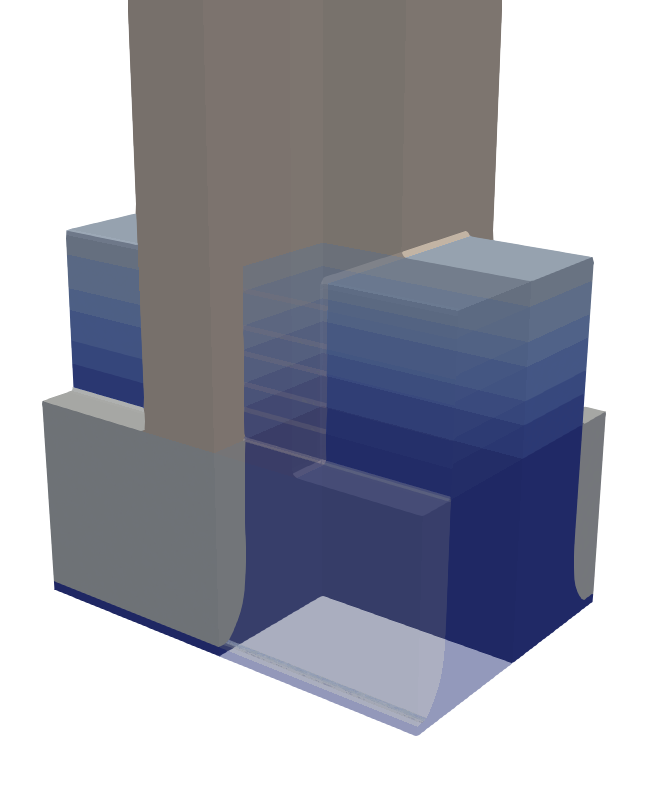
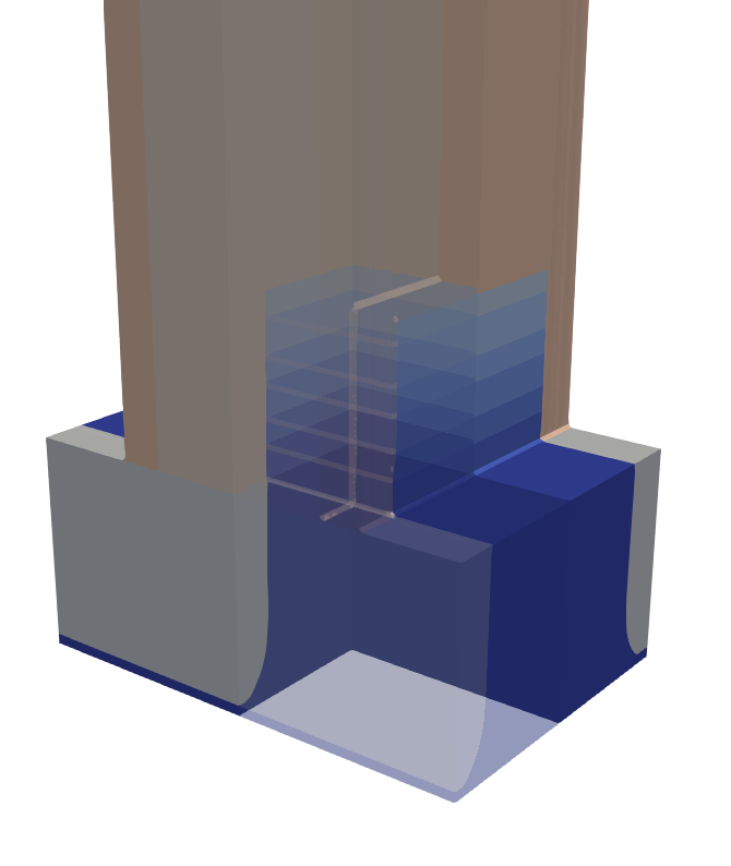
Emulation models were applied consecutively to generate a 22 nm FinFET consisting of two fins rather than a single one, which leads to better electrical characteristics of the device [280]. The exact models carried out are listed in Table 5.6, referring to the structures shown in Fig. 5.23, which resulted after critical process steps were conducted. Models written in bold text are executed using iterative advection rather than geometric advection.
| Fabrication step | Applied model |
| Fin Mask | Mask |
| SADP | Geometric Deposition, Geometric Etch |
| Mask Removal | Delete Material |
| Fin Patterning | Geometric Etch |
| SADP Mask Removal | Delete Material |
| STI Deposition, CMP | Geometric Deposition, CMP |
| STI Etching | Geometric Etch |
| High-k Deposition | Geometric |
| Dummy Gate Deposition, CMP | Geometric, CMP |
| Dummy Gate Mask | Mask |
| Gate Patterning | Geometric Etch |
| Gate Mask Removal | Delete Material |
| Spacer Deposition | Geometric Deposition |
| Spacer Patterning | Geometric Etch |
| Fin Recess | Geometric Etch |
| S/D Epitaxy | SLLF Epitaxial Growth |
| ILD Deposition, CMP | Geometric Deposition, CMP |
| Dummy Gate Removal | Delete Material |
| Gate Metal Deposition | Geometric Deposition |
| Gate Contact Deposition | Geometric Deposition |
| Chemical mechanical planarisation (CMP) | CMP |
Table 5.6: Sequence of process steps used to generate the 22 nm FinFET structure and the models used. Geometric deposition and etching refers to a model executed by the algorithm presented in Section 2.4.3, while SLLF Epitaxial Growth refers to the physical epitaxial model presented in Section 5.1.2.1. CMP is modelled by simply clipping all level sets by a plane using Boolean operations.
The final structure clearly shows all the relevant features, including the crystal facet dependent shape of the epitaxially grown S/D contacts. The epitaxial growth is the only process step emulated using iterative advection, as the temporal evolution of the crystal facets dominates the final geometry, which cannot be represented appropriately using geometric advection. However, since no expensive MC ray tracing simulations are required, only the computational cost of the SLLF advection scheme is incurred. Therefore, the entire structure could be generated in a matter of a few minutes, which allows for changes in the process flow to be made quickly and effectively, resulting in a structure that could be used for subsequent device simulation within a design technology co-optimisation (DTCO) flow straight-forwardly.
FinFETs have been the standard design for modern 3D transistors up to the most recent technology nodes [281]. Due to the complex 3D arrangement, parasitic resistances and capacitances can become a problem for stable device operation [282]. As these properties are strongly dependent on the exact geometry of the transistor, the geometries resulting from a simulation should be as accurate as possible. For a full description of the electric characteristics of devices, the entire circuit must be considered, so a full static random access memory (SRAM) cell of the 5 nm technology node was simulated.
Since parasitic resistances and capacitances mostly originate from the S/D regions, simulation time and effort can be saved by only physically simulating these sections of the device, while emulating all other fabrication steps [283]. The process flow for the SRAM cell is listed in Table 5.7, with critical process steps for the formation of the S/D regions shown in bold text.
| Fabrication step | Applied model |
| Fin Mask | Mask |
| Fin Patterning | SF6/CH2F2 Plasma Etching |
| STI Deposition, CMP | Geometric Deposition, CMP |
| STI Etching | Geometric Etch |
| Dummy Gate Depo, CMP | Geometric Deposition, CMP |
| Dummy Gate Mask | Mask |
| Gate Patterning | Geometric Etch |
| Spacer Deposition | Geometric Deposition |
| ILD Deposition, CMP | Geometric Deposition, CMP |
| Once for NMOS and PMOS eachOnce for NMOS and PMOS eachOnce for NMOS and PMOS each | |
| Mask NMOS/PMOS | Mask |
| PMOS/NMOS ILD Etch | Geometric Etch |
| Spacer Etch | CH3F Plasma Etching |
| Fin Recess | Selective Dry Etch |
| S/D Epitaxy | SLLF Epitaxial Growth |
| ILD Deposition, CMP | Geometric Deposition, CMP |
| Dummy Gate Removal | Geometric Etch |
| HKMG Deposition, CMP | Geometric Deposition, CMP |
Table 5.7: Process steps used to generate the final SRAM structure and the corresponding modelling approaches. The bold text shows which steps were applied using physical models.
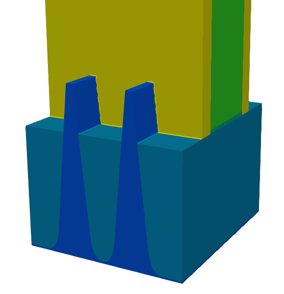
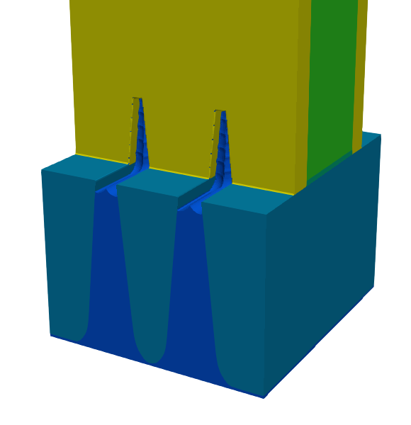
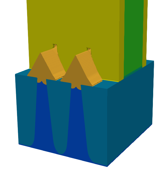
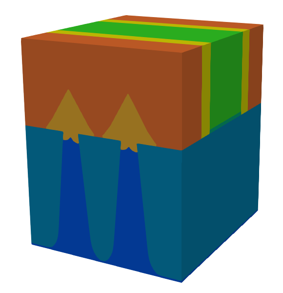
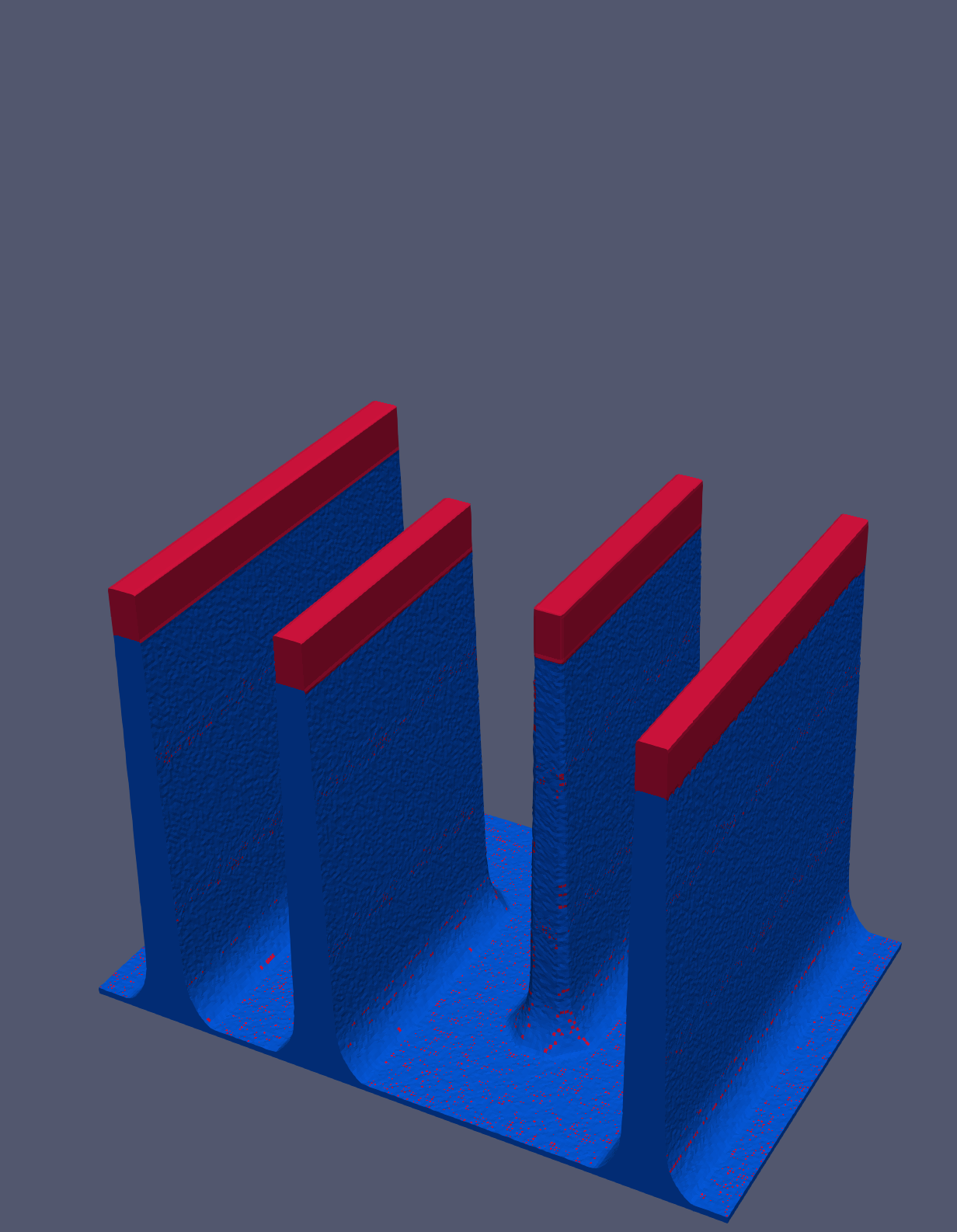
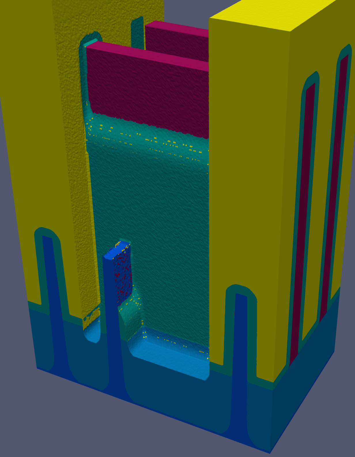
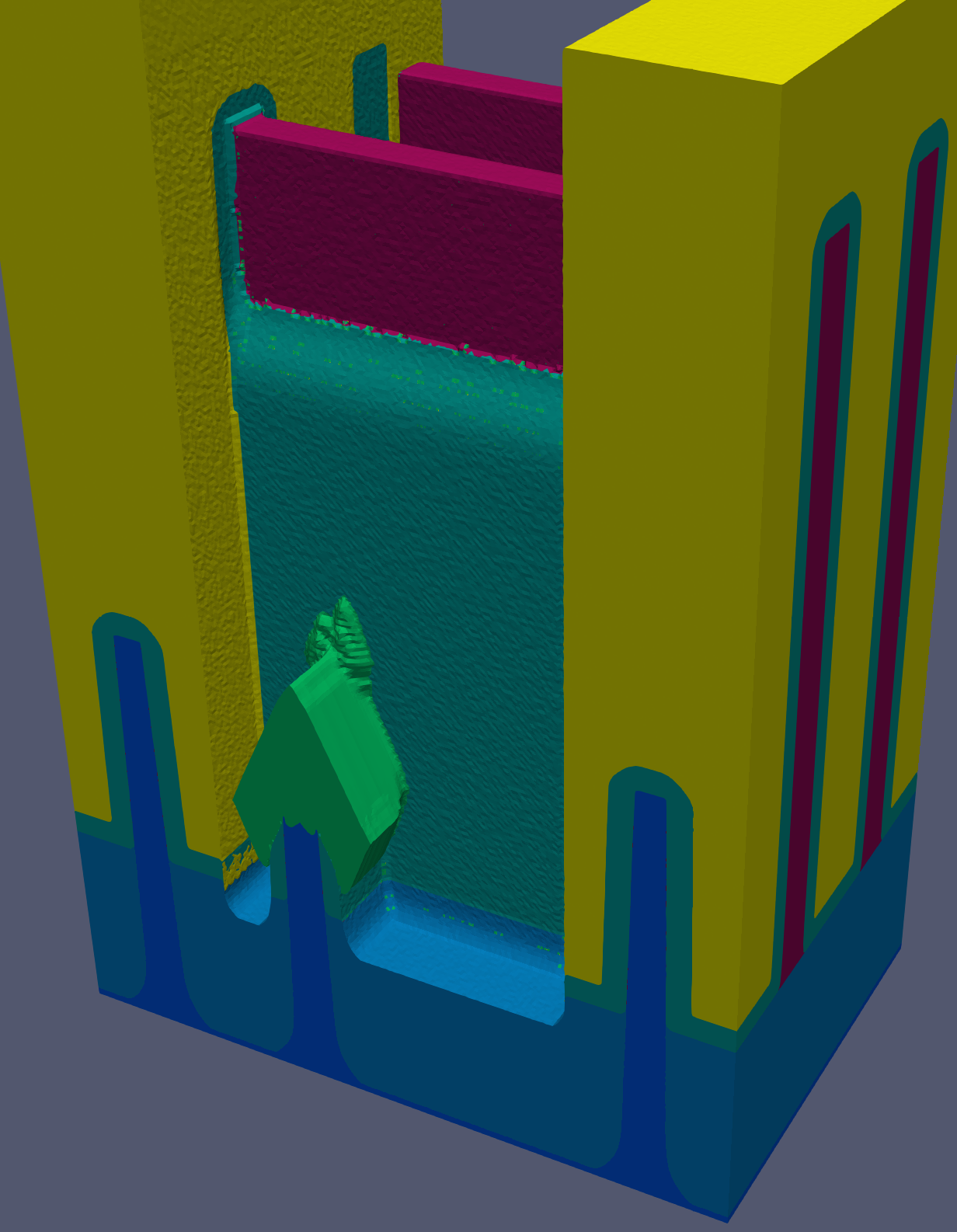
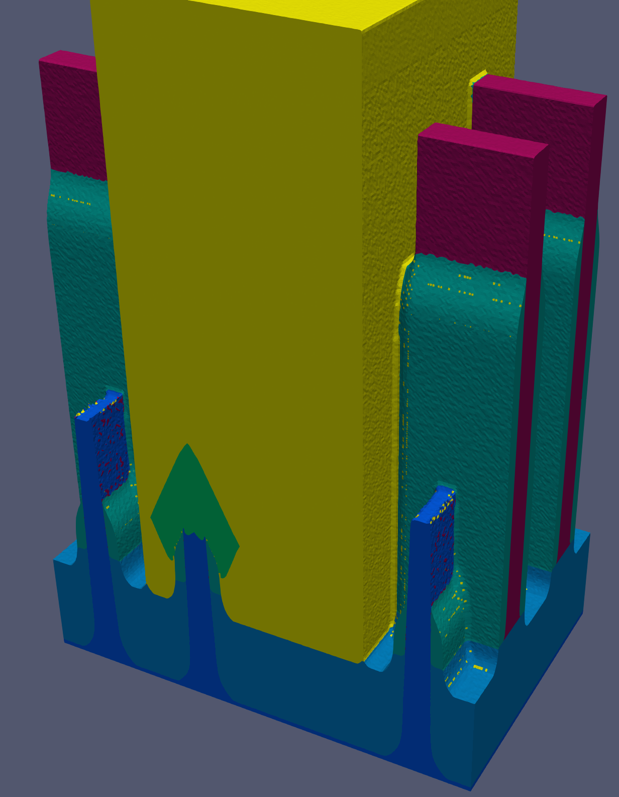
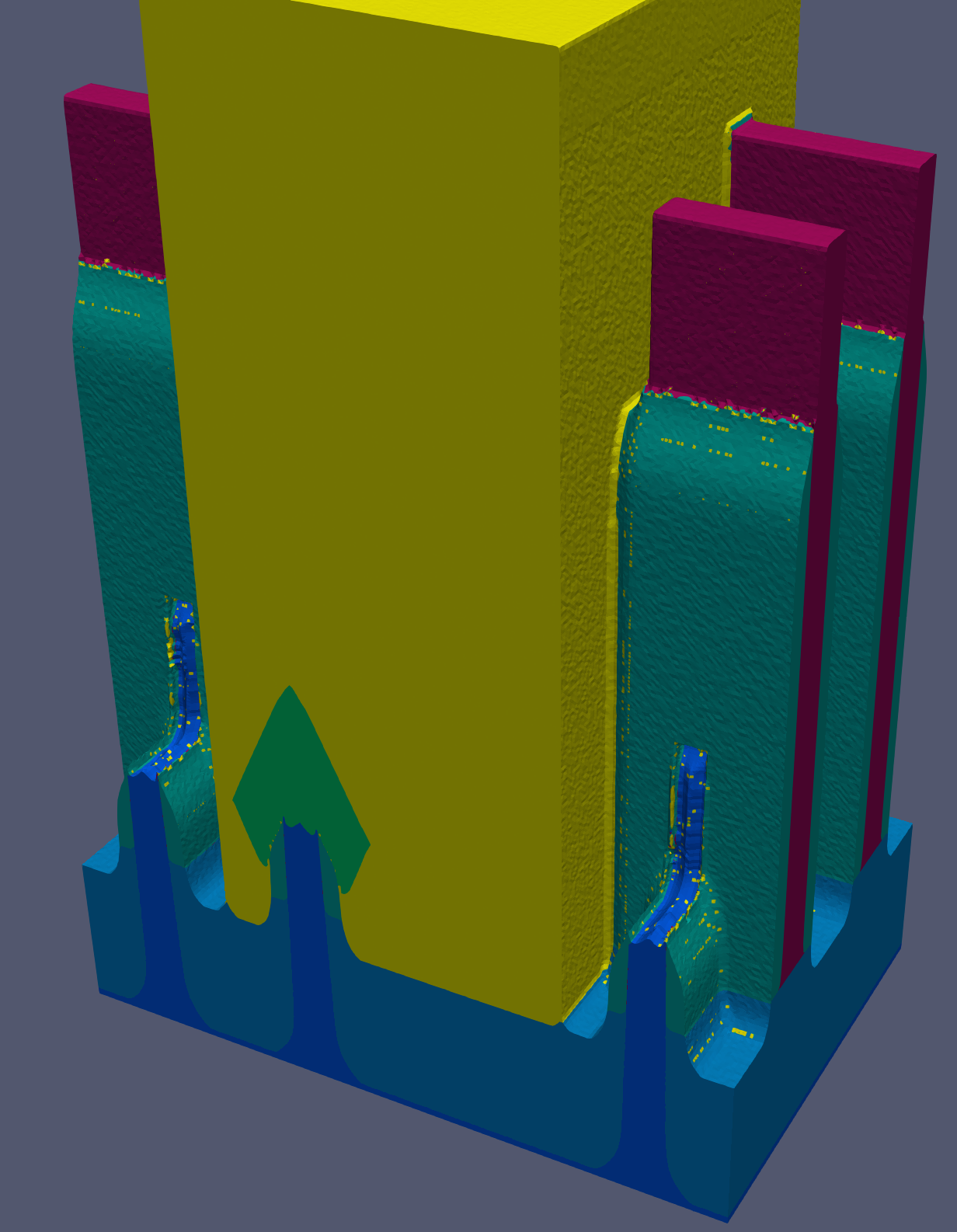
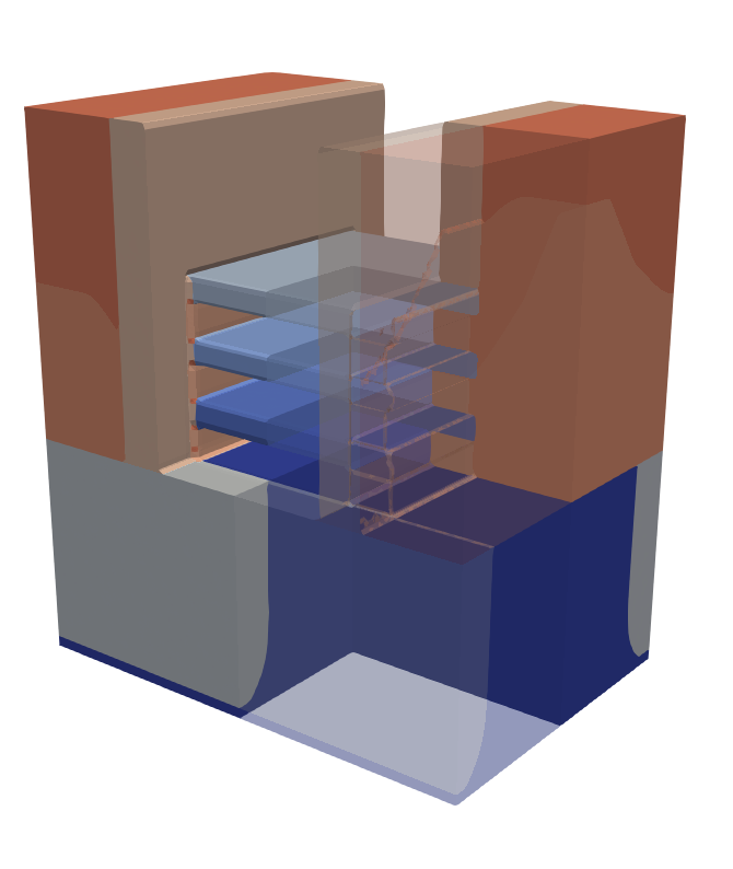
The first process step of interest is the fin patterning, which is simulated using MC ray tracing with the chemical model for CH3F presented in Section 5.1.4.1. All other critical process steps are applied during S/D formation, which means that they must be repeated once for the NMOS and once for the PMOS regions of the cell. The second critical step is CH3F plasma etching of the gate spacer whereby the top of the fin is exposed. Next, the fin is etched in a SF6/CH2F2 plasma to create a clean surface for the subsequent epitaxial growth of the S/D contacts. The SEG of silicon on top of the exposed fin is simulated using the model presented in Section 5.1.2 using the empirical rates presented in [100]. The geometries resulting from these critical process steps are shown in Fig. 5.24 and clearly show the physical behaviour of the specific process steps, which can only be appropriately described using these sophisticated models.
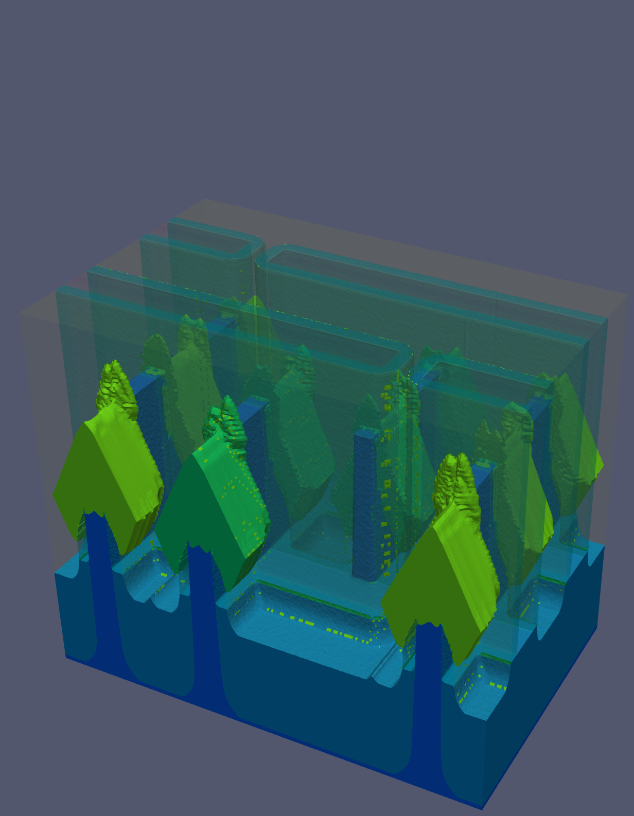
Figure 5.24: (a)-(g) SRAM structure after the fabrication steps with physical models, highlighted in bold in Table 5.7. (h) Final SRAM structure, with high-k dielectric and metal gate (HKMG), spacer and ILD transparent to show the structure of the fins and S/D regions. ©2021 IEEE [283]
Since only a small number of processes actually affect the exact geometry of the S/D regions, only these processes need to be simulated using computationally expensive physical models. All other process steps can be emulated using the highly efficient geometric advection algorithm presented in Section 2.4.3. Therefore, the entire SRAM structure can be generated in less than 16 minutes, where more than 85% of the total simulation time is consumed by the physical models, as shown in Table 5.8. Again, models in bold text indicate physical models, which clearly require the vast majority of computational effort. Therefore, intricate process specific properties influencing the electric properties of the devices in a circuit can be simulated for the entire cell in a reasonable time frame on a consumer desktop computer.
| Fabrication step | Simulation Runtime |
| Fin Mask | 0.1 s |
| Fin Patterning | 186.8 s |
| STI Deposition, CMP | 0.3 s |
| STI Etching | 13.5 s |
| Dummy Gate Deposition, CMP | 0.3 s |
| Dummy Gate Mask | 0.1 s |
| Gate Patterning | 24.4 s |
| Spacer Deposition | 2.8 s |
| ILD Deposition, CMP | 0.3 s |
| Once for NMOS and PMOS eachOnce for NMOS and PMOS eachOnce for NMOS and PMOS each | |
| Mask NMOS/PMOS regions | 0.2 s / 0.1 s |
| PMOS/NMOS ILD Etching | 60.7 s / 76.6 s |
| Spacer Etching | 204.7 s / 225.9 s |
| Fin Recess | 60.6 s / 63.6 |
| S/D Epitaxy | 28.8 s / 28.2 s |
| ILD Deposition, CMP | 0.3 s / 0.4 s |
| Dummy Gate Removal | 0.1 s |
| HKMG Deposition, CMP | 6.7 s |
| Emulation Models | 2 min 22.8 s |
| Physical Models | 13 min 18.6 s |
| Total Runtime | 15 min 41.4 s |
Table 5.8: Runtime for the simulation of each modelled process step. Physical models are shown in bold text. The simulation was carried out on an AMD Ryzen3950X processor and took less than 16 minutes to complete, where more than 85% of the simulation time was consumed for the evaluation of the physical models.
Since its introduction in the 22 nm technology node, the FinFET has been steadily scaled down to reach ever smaller dimensions. However, electrostatic control over the channel of FinFETs is not ideal and the scaling of FinFETs is reaching its limit. Hence, for technology nodes beyond the 5 nm node, the use of gate all-around (GAA) transistors has been proposed [284, 285].
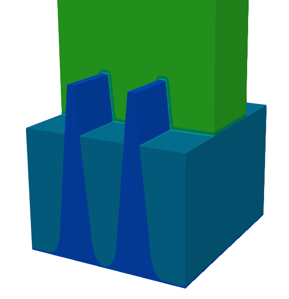
A GAA transistor was emulated using the process flow described in [285]. The models used to generate the structure are listed in Table 5.9, with key processes shown in Fig. 5.25. Due to the wide nano sheets, existing masking technology can be used without reaching critical process limits [286]. Additionally, the stacking of several sheets, which increases power, does not affect the footprint of the structure. Therefore, the electrical characteristics can be improved without requiring larger transistors, as would be the case when additional fins are required in a FinFET.
The individual process steps required to build this type of transistor are very similar to the FinFET process flow, with a few additional steps, as listed in Table 5.9. First, a multilayered stack of SiGe/Si/SiGe/Si is grown epitaxially, as shown in Fig. 5.25a. The silicon layers will form the nanosheet channels of the final device, so the layer width is equivalent to the height of the nanosheets [287]. Subsequently, the same process steps as in FinFET production are used for fin generation: STI and dummy gate formation. However, after the gate spacer is formed, a selective etch process is used to create an under etch in the SiGe/Si stack, as shown in Fig. 5.25d. This under etch will be used to deposit the inner spacer shown in Fig. 5.25e, which isolates the S/D region from the gate and therefore should be as wide as the gate spacer [288]. During the RMG process, the SiGe layers in the channel region are selectively removed to expose the stacked silicon nanosheets, as shown in Fig. 5.25h. Finally, the conventional HKMG is deposited on the suspended nanosheets to form gate contacts all around the channels, leading to optimal electrostatic control [202]. The final structure is shown in Fig. 5.25i, clearly showing the HKMG wrapped around the nanosheet channels, as well as the characteristic crystal facets in the epitaxially grown S/D regions.
| Fabrication step | Applied model |
| SiGe/Si/SiGe/Si/SiGe/Si Epitaxy | Geometric Deposition |
| Fin Mask | Mask |
| SADP | Geometric Deposition, Geometric Etch |
| Mask Removal | Delete Material |
| Fin Patterning | Geometric Etch |
| SADP Mask Removal | Delete Material |
| STI Deposition, CMP | Geometric Deposition, CMP |
| STI Etching | Geometric Etch |
| Dummy Gate Deposition, CMP | Geometric, CMP |
| Dummy Gate Mask | Mask |
| Gate Patterning | Geometric Etch |
| Gate Mask Removal | Delete Material |
| Spacer Deposition | Geometric Deposition |
| Spacer Patterning | Geometric Etch |
| Fin Recess | Geometric Etch |
| SiGe Etch for Inner Spacer | Geometric Etch |
| Inner Spacer Formation | Geometric Deposition, Geometric Etch |
| S/D Epitaxy | SLLF Epitaxial Growth |
| ILD Deposition, CMP | Geometric Deposition, CMP |
| Dummy Gate Removal | Delete Material |
| High-k Gate Dielectric Deposition | Geometric Deposition |
| Gate Metal Deposition | Geometric Deposition |
| Gate Contact Deposition | Geometric Deposition |
| CMP | CMP |
Table 5.9: Emulation models used to simulate the fabrication of a GAA FET anticipated for applications beyond the 5 nm technology node.