|
GaN is considered as a promising semiconductor due to its wide bandgap, high breakdown field, high electron mobility and sheet carrier density making it ideal for power applications. Si substrate is used due to its low cost and wide availability. The problems of the integration of GaN thin films on Si substrates arise due its specific physical and chemical properties.
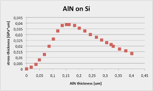
It has been demonstrated that it is not possible to grow monocrystalline GaN directly on Si substrates due to the large lattice, thermal, and chemical potential mismatch. For these reasons different kinds of buffer layer schemes between Si and GaN have been invented. The simplest buffer is an AlN thin layer. Another solution is a graded AlGaN layer. In all cases, the growth mode of a III-nitride thin layer upon a Si substrate is the so-called island growth, also known as the Volmer-Weber growth. It implies that a polycrystalline buffer layer is created and several columnar grains separated by low-angle grain boundaries and domain walls compose it. Dislocations composing these low-angle grain boundaries propagate into the layers above, included the GaN layer, affecting its electronic and optical properties.
I investigate the Volmer-Weber growth of the III-nitrides on silicon and the subsequent low-angle grain boundaries formation using analytical models based on energetic minimization criterions and with the aid of mechanical simulations performed by a finite element method software.
Additional dislocations are formed when GaN is grown above the buffer layer. This happens through the Frank-VanDerMerwe growth. In this situation, dislocations are created when the GaN thickness is higher than a critical value. Several criterions, like the People-Bean and the Matthews-Blakeslee methods, allow prediction of the critical thickness value. The aim is to describe the relaxation process due to the dislocations' dynamics by means of mathematical models and combine these results with, firstly, the influences of the Volmer-Weber grown buffer layer and, secondly, with the inverse piezoelectric effect — that characterizes the III-nitride's — influences.
|