|
The continued miniaturization of Si-integrated devices in CMOS
technology is approaching the physical limits. To meet the
requirements of the international technology roadmap for semiconductors, the innovation of novel nano-electronic devices are expected. Graphite-related materials such as
fullerenes, carbon nanotubes, and graphene have been extensively
studied in recent years due to their exceptional electronic,
opto-electronic, and mechanical properties. Graphene, a one-atomic
carbon sheet with a honeycomb lattice, is a gapless material that has attracted significant
attention due to its unique physical properties. This material shows
an extraordinarily high carrier mobility and is considered to be a
potentially high speed transistor material. To induce a bandgap, graphene sheets can be patterned into
ribbons. Depending on the width and the chirality, a Graphene
NanoRibbon (GNR) can have semiconducting or metallic properties. The
bandgap of a semiconducting GNR is inversely proportional to its
width. In order to obtain an energy bandgap larger than 0.1eV, which
is essential for electronic applications, the width of the GNR must be
scaled below 10nm. In this regime line-edge roughness is the dominant
scattering mechanism.
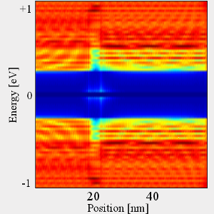
To model carrier transport of carriers in GNRs, the Non-Equilibrium Green's
Function (NEGF) formalism and an atomistic tight-binding model have
been employed. We model the effect of line-edge roughness using a
non-perturbative approach. In this method, many GNR samples with rough
edges are generated using a Gaussian or exponential distribution and
then an ensemble average is calculated. Line-edge roughness at the
two edges can have some degrees of correlation. Cross correlation
between two random processes is described by a correlation coefficient
which lies between -1 and +1. A correlation coefficient of +1 can be achieved in between the two edges of unzipped carbon nanotube GNRs,
whereas the correlation coefficient for GNRs obtained from other methods is nearly zero. Our
studies show that this correlation can play a significant role on the
electronic properties of GNRs. In GNRs with un-correlated roughness,
the electronic bandgap is strongly modulated by line-edge
roughness. In GNRs with a correlation factor of +1, the width of the
ribbon remains nearly constant and the bandgap is only weakly
affected.
|