|
A Level Set simulator for moving boundaries, which has been developed at this institute, has been enhanced to include several modern semiconductor processing techniques. Using Level Sets to identify and advance wafer surfaces during various deposition and etching steps has previously been implemented. However, due to the constant advancement of semiconductor processing techniques and the constantly shrinking technology node, there is a growing need for a simulation tool which is able to handle these novel processes. A method for simulating novel techniques which enable cost-effective miniaturization for reduced technology nodes has been implemented within the Level Set environment. These processes include nanolithography using an Atomic Force Microscope (AFM) in tapping and non-contact mode, the deposition of thin films using the spray pyrolysis technique, and the etching of intermittent silicon and silicon dioxide layers for the generation of three-dimensional memory holes for Bit Cost Scalable (BiCS) memories.
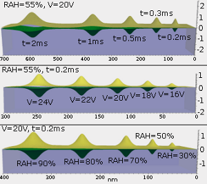
The local anodic oxidation of silicon surfaces with an AFM produces nanosized patterns on a silicon wafer using a localized charged needle. The technology has been developed in order to tackle the limited miniaturization potential of current photolithographic techniques. A technique is introduced which models the changing silicon topography as the silicon dioxide pattern is applied to the wafer. The charges required to initiate oxidation arise due to the application of a strong electric field between the AFM needle tip and the silicon wafer surface. The electric field is analyzed and the charge density on the wafer surface is calculated. Using Monte Carlo techniques this charge density is converted to a particle distribution, which is then applied to the velocity field of the oxide surface. The surface evolutions caused by the electric field are then represented as a Level Set surface evolving under a velocity field driven by the electric field and the chemical reaction at the wafer surface.
A spray pyrolysis deposition model is also developed and implemented within the Level Set framework. This processing technique enables the deposition of thin films for applications such as gas sensors and solar cells. Two models for the topography modification due to spray pyrolysis deposition are presented; with an electric and a pressure atomizing nozzle. When an electric nozzle is used, the droplets' flight towards the wafer is governed by the strong electric field in the region. Complex motion equations are implemented to calculate where the droplets contact the wafer surface, based on all external forces acting on the droplet: gravitational, Stokes, electrical, and thermophoretic. The resulting film growth is modeled as a layer by layer deposition of the individual droplets which reach the wafer surface. A pressure nozzle does not include a strong electric field and the droplets are viewed as traveling through the air as a flux, finally reaching the surface and depositing in a CVD-like process.
Similarly, EEPROM memory cells can not be miniaturized further with the current processing techniques. Therefore, three-dimensional structures are being introduced in order to increase the number of available memory cells without increasing the area required. A model for BiCS memory hole etching is implemented in the given Level Set framework as a combination of silicon and silicon dioxide etching steps.
|