|
Nowadays MOSFET have characteristic length in the nanometer regime, for example the
recently presented Intel FinFETs have a gate length of L = 22nm. Accompanying the advantages of higher operation frequency and lower
power consumption are the parasitic effects, which also have to be considered. In
particular, Bias Temperature Instabilities (BTI) have become a
major reliability issue.
The recently introduced Time Dependent Defect Spectroscopy (TDDS)
takes advantage of the fact that nano-scaled devices only exhibit a
handful of defects. Each single defect can capture/emit a carrier
from/into the drain current of the conducting channel. The carrier
emission events are observed as a change in the drain current during
the operation and are also visible as a change in the threshold voltage of
the MOS transistor. As a consequence, the carrier capture and emission
events are visible as discrete steps in the drain current. In
contrast, in large area devices, a continuous degradation or recovery
is observed.
An experimental challenge is to measure nanoampere drain currents
with reasonable resolution in order to observe small discrete
carrier capture and emission events in the drain current. Also, a high
bandwidth (high operation speed) of the measurement circuit is
necessary.
For the evaluation of the TDDS data, a sophisticated analysis
algorithm has been designed. The main focus was on developing an
algorithm that can detect positive and negative changes in a
non-uniformly sampled drain current (or more commonly, in non-uniformly
sampled measurement data). The data analysis algorithm is based on the
bootstrapping technique combined with the cumulative sum chart
statistics.
By using the new algorithm, both, single capture/emission events and
Random Telegraph Noise (RTN) can be studied within the framework of
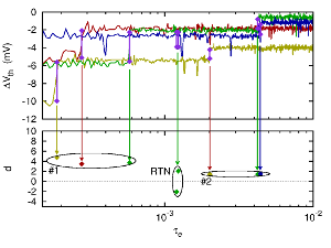
TDDS. The spectral maps obtained from the TDDS measurement and a
subsequent signal analysis shows the RTN events symmetrically arranged
around the x-axis while single detrapping events appear as a cluster
(see figure). Each cluster represents a collection of carrier
detrapping events of a single defect for repeated NBTI stress and
recovery measurements. In particular, each cluster acts as the
fingerprint of a single defect of the MOS transistor.
Under certain bias conditions RTN can occur randomly. With the new
method we can perform conventional RTN analysis as well as the
analysis of single defects, which are the cause for the permanent degradation.
|