|
Three-dimensional Integrated Circuits (3D ICs) are chips that extend the traditional integration into the third dimension. The electronic components in these chips are not only placed side by side, but also above each other on two or more layers. In these configurations shorter connections between components are possible resulting in lower signal delay and energy consumption compared to 2D ICs. This may provide the opportunity to develop faster systems with a longer battery life, in addition to being smaller on account of the reduced circuit board area.
Through Silicon Vias (TSVs) are interlayer connections. These connections do not run over the edges of the connected layers but directly through the silicon substrate. Therefore the usage of TSV will lead to a further shortening of the connections. Also these connections need no interposer layer resulting in thinner 3D IC structures. Like all interconnects, these also suffer from electromigration, which, besides other degenerative processes, limits their lifetime.
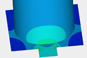
Finite element simulations were carried out to distinguish the highest current density regions. Figure 1 depicts the result of these simulations. The highest current densities are located in the overlapping region between the different metals of the conductor. Four different effects influencing the electromigration degeneration have to be addressed. The first three effects are vacancy diffusion inside the monocrystalline grains, along the grain boundaries of one metal and along interfaces between different materials. The fourth effect is the segregation of vacancies in the interface region between different conducting materials. Thus, the question arises which of these has the highest influence on the lifetime reduction of TSV structures and are there techniques to reduce them.
To study these effects a two-stage approach is applied. For a better understanding of the atomistic processes, Molecular Dynamic simulations (MD) are performed. Thereby the atoms are modeled obeying Newton's differential equations for a model potential. This model potential has to be verified and, if necessary, adjusted by ab-initio simulations. The parameters extracted from MD can be used to carry out continuum mechanical based electromigration simulations.
|