|
Silicon NanoWires (NWs) and ultra-thin layers are promising
building blocks for electronic and thermoelectric devices.
Length scale and orientation provide additional degrees of freedom in
engineering the electronic and thermal transport properties.
We use the sp3d5s*-SO tight-binding model and Boltzmann transport
theory, including all relevant scattering mechanisms, to investigate
the thermoelectric properties of Si NWs. It is found that
structural quantization below 10nm can severely affect the electronic
properties of NWs by changing the curvature of the bands and
altering degeneracies through valley and subband splitting. Specifically
for p-type NWs, it was found that at large diameters, NWs oriented
along the three principle orientations [100], [110] and [111], have a
similar thermoelectric power factor. A large anisotropy in the
thermoelectric power factor was found, however, for smaller
diameters. As the diameter is scaled to 3nm, the power factor of the
[111] and secondly the [110] NWs largely increases, whereas that of
the [100] NWs remains low. This behavior originates
from confinement-induced large curvature variations in the
electronic subbands. In addition to electron transport we also investigated
phonon transport in Si nanostructures. Si NWs with diameters in
the range 1-10nm are considered. The lattice dynamics are
modeled using the modified valence force field method, the
ballistic thermal conductance is calculated using the Landauer
transport formalism.
The phonon group velocity and thermal conductance can vary by a factor
of two depending on the geometrical features of the channel. Group
velocity and thermal conductance is highest in the <110> NW and lowest
in and the <111> NW. The <111> orientation is the most suitable
for thermoelectric devices based on Si NWs. We also consider
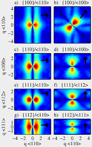
ultra-thin Si layers of major surface orientations {100}, {110},
{111}, and {112}. We find that the ballistic thermal conductance in the
thin layers is anisotropic, with the {110}/<110> channels exhibiting
the highest and the {112}/<111> channels the lowest thermal
conductance. The resulting ratio is about two.
To model electronic transport in Quantum Cascade Lasers (QCL)
and Quantum Cascade Detectors (QCD) we resort to the Pauli master equation.
An efficient Monte Carlo (MC) simulator as part of
the Vienna-Schrödinger-Poisson (VSP) simulation framework
has been further enhanced.
Several band structure models such as 2-band k·p or 4-band k·p
can be combined with different in-plane dispersion relations used
in the transport calculation. A model for stimulated emission and
absorption of photons has been implemented.
The simulator has been used to design and optimize the first
functioning bi-functional QCL and QCD device.
In mid-infrared and terahertz devices,
novel types of optical guides and resonators are commonly found,
such as ring cavities, micro-discs, photonic crystals, super-crystals
and micro-antennas. Of particular interest are Photonic Crystal (PHC)
cavities. This
allows investigating the properties of a large finite PHC based on the
analysis of a single unit cell. In our work a real-space approach is
used. The periodicity is
explicitly ensured by connecting the mesh vertices that lie on
opposite surfaces of the unit cell. Thus, the unit cell can be made
periodic only in certain spatial dimensions while different boundary
conditions may be applied in the remaining dimensions.
The real-space approach with mixed boundaries gives us the possibility
to analyze PHC slabs. To capture this radiative dissipation effect we apply
periodic boundary conditions in the horizontal plane and absorbing boundary
conditions below and above the slab. Doing so, we obtain a complex photonic
band structure which contains wavevector-dependent information about
radiative losses for every PHC mode.
To model carrier transport in Graphene NanoRibbons (GNRs)
the Non-Equilibrium Green's Function (NEGF) formalism
and an atomistic tight-binding model have
been employed. We investigate the effect of line-edge roughness using a
non-perturbative approach. In this method, roughness is applied to
many GNR samples using a Gaussian or exponential distribution and then
ensemble averages are computed. Line-edge roughness at the two edges
can have some degrees of correlation. In GNRs obtained by
unzipping of carbon nanotubes the correlation coefficient between
theses two edges is +1, whereas that for GNRs obtained from other
methods is nearly zero. Our studies show that this correlation can
play a significant role on the electronic properties of GNRs. In GNRs
with un-correlated roughness, the electronic bandgap is strongly
modulated by line-edge roughness.
|