|
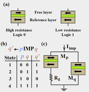
Non-volatile logic is a promising solution to overcome the standby power issue, which has become a prominent concern due to high leakage currents as CMOS technology continues to reduce in size. Magnetic Tunnel Junction (MTJ) technology (figure 1a) has great potential because of unlimited endurance, CMOS compatibility, and fast switching speed. Furthermore, Spin-Transfer Torque (STT) switching technique eliminates the difference between reading and writing in conventional MTJs and shows great promise for the next generation of highly scalable and low power non-volatile memory technology. We propose a novel circuit topology for STT-MTJ-based spintronic logic gates (figure 1b) which provides conditional switching behavior on the target (output) MTJ Mq, which corresponds to a fundamental Boolean logic operation called Material Implication (IMP) (figure 1c). This extends non-volatile electronics from memory to logical computing applications and opens the door for zero-standby computation systems and shifts away from the Von Neumann architecture by eliminating the need for transfer data between separate memory and logic units.
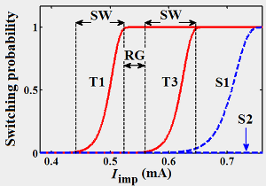
An MTJ device contains two ferromagnetic layers separated by a tunneling barrier (figure 1a). The magnetization of one layer (reference layer) is pinned, while the magnetization of the second free layer can be switched freely using the STT effect. The electrical resistance of the device depends on the relative orientation of the magnetization directions of the ferromagnetic layers. The parallel (P) magnetization state results in a low-resistance state (RP; logic 1) across the barrier, while the antiparallel (AP) alignment places it in a high-resistance state (logic 0; RAP). The resistance modulation is described by the Tunnel MagnetoResistance (TMR) ratio, defined as (RAP-RP)/RP. By applying Iimp, the target MTJ (MT) switches from high (logic 0) to low resistance state (logic 1) only when both MTJs are initially in high resistance state (State 1). Due to the reliable gap (RG), the source MTJ (Mp) is left unchanged for all possible initial logic states (figure 1b). Figure 2 shows the switching dynamics of Mp and Mq as a function of Iimp plotted for Rg=900Ω. For Iimp within the RG, which is opened between the Switching Windows (SWs) of the desired and undesired switching events (q1 and q3), correct logic behavior is ensured. To optimize device functioning, reliable IMP logic behavior needs a high enough TMR ratio since the modulation of the current passing through the target MTJ required for STT-switching, thus the width of RG, increases with TMR ratio.
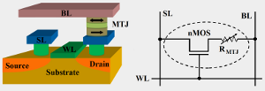
Due to easy integration of the MTJ on top CMOS circuits, by replacing the MTJ devices with 1T/1MTJ cells (figure 3), the IMP logic gates can be extended to large-scale non-volatile magnetic circuits. Since the 1T/1MTJ cell is the basic element for STT-MRAMs, this concept provides magnetic logic circuits that can also be used for random-access memory applications. In combination with low to high MTJ resistance switching (FALSE operation), IMP forms a computationally complete logic basis. For example, an IMP-based full adder design involves 27 subsequent FALSE and IMP operations on 6 1T/1MTJ cells. As compared to previously proposed magnetic full adders, since the 1T/1MTJ cell is used as both memory and the main computing element, IMP-based logic eliminates the need for CMOS-based logic elements and intermediate circuitry including sensing amplifiers. Logic circuits that simultaneously exhibit low power consumption, high logic density, and high speed operation can thus be designed.
|