|
Three-dimensional (3D) integration has become a very promising technology for
the microelectronics industry. One key component of 3D integration to achieve
these features is the Through Silicon Via (TSV). The TSV consists of a
conducting via fabricated through a silicon substrate, which connects
components of different integration levels. Reliability is a critical issue
for new emerging technologies such as TSVs. In particular, electromigration
is one of the main reliability concerns in back-end of line
interconnects.
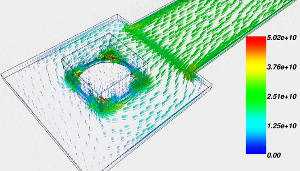
Figure 1 shows the electron current density distribution at the TSV bottom in
the presence of a void. The electron flow is displaced towards the corners of
the via, which leads to current crowding in this region. The void causes a
reduction of the effective conducting area, increasing the resistance of the
interconnect structure. In addition, imperfections on the bottom of the TSV
are typically introduced during the fabrication process. For example, control
of the thin barrier layers at the bottom of the TSV is a key issue, which can
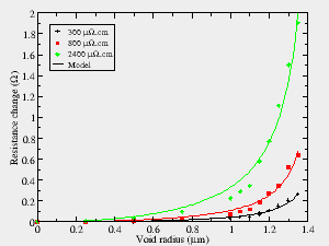
result in a high variation of the barrier layer resistivity. The impact of
such a variation on the electromigration induced resistance change of the
interconnect is shown in figure 2. The large dispersion of the effective barrier
resistivity significantly affects the structure resistance, leading to a large
resistance increase, even when the void radius is smaller than the via
dimensions.
We have proposed a model which satisfactorily describes the resistance
increase in the presence of a small void under the TSV. In addition, we
verified that upon triggering the line failure, this mechanism forms an
extrinsic, early failure mode, which acts primarily at low cumulative
percentiles. Considering that the reliability assessment of an interconnect is
typically performed at very low failure percentiles, the early failures
described above might be the main relevant mechanism for electromigration
failure in copper dual-damascene lines ending in TSV structures.
|