|
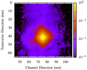
Decades ago Andersson et al. [1] extensively studied the occurrence of gate current fluctuations in MOS tunnel diodes. As Random Telegraph Noise (RTN) in the drain current has emerged as a serious reliability issue for MOS devices, recent investigations revealed that the fluctuations in the drain and the gate current can be correlated. The drain noise has also been investigated in the context of the Bias Temperature Instability (BTI) and is traced back to the capture and emission of substrate charge carriers in the gate oxide. It may be argued that the captured charge locally repels the inversion layer, thereby decreasing the direct tunneling current through the gate oxide. This effect has been investigated using Non-Equilibrium Green's Functions (NEGF) simulations for a series of random dopant configurations. In the worst case, they predict a change in the gate current of less than 1% (see figure 1) while measurements yield values around 8%. As a consequence, this electrostatic effect can be ruled out as an explanation for the gate current fluctuations.
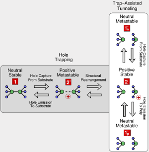
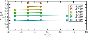
In the related field of BTI, a multistate defect model has been recently proposed and is the only one that is consistent with a multitude of experimentally observed features: (i) The RTN/BTI capture and emission times are uncorrelated. (ii) The capture times show a strong field dependence ascribed to different curvatures in adiabatic potentials. (iii) Their frequency dependence is explained by the introduction of an additional metastable state. In this model, the TAT current consists of two nonradiative multiphonon transitions, namely, hole capture from the substrate (from state 1' to state 2) followed by hole emission to the poly gate (from state 2 back to state 1'). As shown in figure 2, the resulting TAT current only occurs for the positive charge state of the defect and can be switched on by hole capture (from state 1 to state 2) or turned off again via hole emission (from state 2 to state 1). figure 3 demonstrates that the multistate model yields the correct field and temperature dependence of the gate current fluctuations while still fitting the RTN/BTI capture and emission time constants. As such, the multistate model provides a comprehensive description of oxide defects causing BTI and gate leakage and thereby further corroborates the validity of this model.
[1] Andersson et al., Phys.Rev.B, 41, 9836-9842 (1990).
|