

Modeling of Defect Related Reliability Phenomena
in SiC Power-MOSFETs
Chapter 3 Defects in SiC Field Effect Transistors
Advances in material and process engineering have enabled the production of pure crystalline Si with negligible distortions to the ideal crystal structure. An ongoing challenge is the deposition of a suitable insulator ensuring a
high quality interface. Although the lattice mismatch at the interface between the bulk Si and its native oxide leads to electrically active defects, i.e. Si dangling bonds or  centers, these can be passivated by hydrogen atoms in a forming gas annealing step, leading to a chemically stable material system. On the contrary, as outlined in Chapter 1, the quality of the SiC crystal available at wafer scale still suffers from stacking faults, dislocations and point defects. Furthermore, the chemical composition of the
SiC/SiO2 interface is less understood, compared to its mature Si/SiO2 counterpart. While forming gas anneals do not show a significant passivation effect in SiC/SiO2 systems, annealing in
nitrogen containing ambients successfully reduces the number of electrically active defects. However, the exact chemical mechanism of this passivation effect is still debated. Within bulk amorphous SiO2, potential
defect candidates have been identified and studied in detail by atomistic simulations employing ab-inito calculations. In this chapter an overview is provided of the relevant defect types and their properties in bulk
SiO2 and at the SiC/SiO2 interface as calculated with Density Functional Theory (DFT). It has to be noted that the widespread terminology suggested by Fleetwood [167], which categorizes defects in interface, border and oxide traps is not strictly followed throughout this
work. This is because a clear separation of the electrically active defects by its spatial distance to the interface, which would require a sub-nanometer resolution characterization, cannot be provided by the experimental extraction
or transient device simulations available.
centers, these can be passivated by hydrogen atoms in a forming gas annealing step, leading to a chemically stable material system. On the contrary, as outlined in Chapter 1, the quality of the SiC crystal available at wafer scale still suffers from stacking faults, dislocations and point defects. Furthermore, the chemical composition of the
SiC/SiO2 interface is less understood, compared to its mature Si/SiO2 counterpart. While forming gas anneals do not show a significant passivation effect in SiC/SiO2 systems, annealing in
nitrogen containing ambients successfully reduces the number of electrically active defects. However, the exact chemical mechanism of this passivation effect is still debated. Within bulk amorphous SiO2, potential
defect candidates have been identified and studied in detail by atomistic simulations employing ab-inito calculations. In this chapter an overview is provided of the relevant defect types and their properties in bulk
SiO2 and at the SiC/SiO2 interface as calculated with Density Functional Theory (DFT). It has to be noted that the widespread terminology suggested by Fleetwood [167], which categorizes defects in interface, border and oxide traps is not strictly followed throughout this
work. This is because a clear separation of the electrically active defects by its spatial distance to the interface, which would require a sub-nanometer resolution characterization, cannot be provided by the experimental extraction
or transient device simulations available.
3.1 Defects in Bulk Silicon Dioxide
Amorphous SiO2 (a-SiO2) has been studied in great detail due to its importance in semiconductor technology. Among electrical, optical and structural properties, a number of electrically active defect
types have been studied using electrical, magnetic resonance or optical characterization methods, as described in Chapter 2. Experimentally,
paramagnetic defects are often characterized by magnetic or spin resonance measurements. Within  -quartz, the so-called
  center, in which the prime denotes that one is electron involved in the measurement signal and 1 evolves from arbitrary enumeration, has been identified by EPR measurements already in the 1950s [168]. The oxygen vacancy (OV), which naturally forms during the oxidation of silicon, with
densities depending on the oxidation process parameters like temperature and pressure, has been suspected early on as a candidate to explain the EPR spectra for
center, in which the prime denotes that one is electron involved in the measurement signal and 1 evolves from arbitrary enumeration, has been identified by EPR measurements already in the 1950s [168]. The oxygen vacancy (OV), which naturally forms during the oxidation of silicon, with
densities depending on the oxidation process parameters like temperature and pressure, has been suspected early on as a candidate to explain the EPR spectra for  centers in a-SiO2 (which is the equivalent to in the crystalline material) [169]. However, it took until the late 1990s to connect the EPR
data with structural properties derived from ab-initio calculations. Thereby an excellent agreement of the experimentally determined hyperfine structure with the calculated OV [170] was obtained. In its neutral state, the two Si atoms with the missing two-coordinated O bind together, thereby forming a Si-Si dimer. If one of the
binding electrons is removed, e.g. by the application of an external electric field, the defect will eventually relax to its stable positive state which can be detected with ESR and EPR measurements due to the spin of the single
remaining electron at the defect site. The defect can exist in multiple states, e.g. in its stable state the Si atom can eventually bind to a back oriented O atom after moving through the plane spanned by the three adjacent O atoms,
thereby forming a puckered configuration, c.f. Figure 3.1 (top) state 1 and 2 [171]. This transition is accomplished via a meta-stable state (1
centers in a-SiO2 (which is the equivalent to in the crystalline material) [169]. However, it took until the late 1990s to connect the EPR
data with structural properties derived from ab-initio calculations. Thereby an excellent agreement of the experimentally determined hyperfine structure with the calculated OV [170] was obtained. In its neutral state, the two Si atoms with the missing two-coordinated O bind together, thereby forming a Si-Si dimer. If one of the
binding electrons is removed, e.g. by the application of an external electric field, the defect will eventually relax to its stable positive state which can be detected with ESR and EPR measurements due to the spin of the single
remaining electron at the defect site. The defect can exist in multiple states, e.g. in its stable state the Si atom can eventually bind to a back oriented O atom after moving through the plane spanned by the three adjacent O atoms,
thereby forming a puckered configuration, c.f. Figure 3.1 (top) state 1 and 2 [171]. This transition is accomplished via a meta-stable state (1  , 2 ) which is reached by a purely thermally activated structural re-configuration. The existence of such meta-stable states is supported by experimental observation of anomalous RTN [76], which justifies the applicability of a four-state NMP model to describe the kinetics of charge capture and
emission of OVs in detail. Additionally, to the EPR signal, the origin of another EPR signal obtained in a-SiO2, the so-called
, 2 ) which is reached by a purely thermally activated structural re-configuration. The existence of such meta-stable states is supported by experimental observation of anomalous RTN [76], which justifies the applicability of a four-state NMP model to describe the kinetics of charge capture and
emission of OVs in detail. Additionally, to the EPR signal, the origin of another EPR signal obtained in a-SiO2, the so-called  , is not fully understood and has been associated with a re-bonded OV or a multi-vacancy defect [169].


Figure 3.1: Oxygen vacancy in different charge states and configurations (top). The neutral (1) and positive (2) stable states are shown together with meta-stable states (1’,2’). The transition from neutral state 1 to positive state 2 occurs upon emission of one of the electrons in the Si-Si bond (2’) and the following structural relaxation, in which the Si atom moves through the plane spanned by the O atoms and bonds to a back-oriented O atom (2). The distribution of +/0 and 0/- charge transfer levels predicted by DFT calculations [77, 172](bottom) renders the OV a potential defect candidate for both NBTI and PBTI in the SiC/SiO2 MOS structure. The AERs (dashed) are calculated for Eox = 5 MV/cm at 3 nm distance from the interface. (partially reprinted and modified from [173])
Note that recent results suggest that the OV is not considered responsible for charging mechanisms related to PBTI and NBTI in Si/SiO2 transistors employing thin insulating layers [173]. To the contrary, the tails of the distributions of their thermodynamic charge transfer levels calculated by DFT are within the energetic range that are scanned in SiC/SiO2 MOSFETs during operation and stress experiments for both BTI regimes. However, the trap-level distribution of the OV appears energetically more favourable in the PBTI regime as shown in Figure 3.1 (bottom). Furthermore, the relaxation energies for the PBTI relevant transitions -/0 and 0/- as extracted from DFT are asymetrically distributed around 2 eV [172], which is within a reasonable range to link to experimentally observable charge transition kinetics and well agrees with NMP parameter ranges extracted from MSM measurements, as will be shown in Chapter 5. High formation energies of about 7.6 eV [172] at low densities of 1 × 10¹⁴/cm3 to 1 × 10¹⁷/cm3 extracted by EPR measurements [174, 175] on the other hand oppose the relevance of OVs for PBTI. However, increased densities could be observed in thicker and deposited oxides. Since the thermal budget for processing SiC MOSFETs is typically higher compared to Si transistors, different densities may be expected.
At oxygen vacancies embedded in a locally partially recrystallized SiO2 structures, the charge-transfer levels (CTLs) for the +/0 transition are shifted towards the oxide valence band edge, as calculated by hybrid functional DFT [176], rendering OVs potential defect candidates responsible also for NBTI in SiC MOSFETs. The shift of the CTL upon the structural change of the OV from the neutral dimer state 1 to its positive state 2 upon hole capture could also explain the positive charge built up upon bipolar stress in p-type MOSCAPs, i.e. long-term NBTI and PBTI subsequently, as suggested by Shen et. al [86]. Hole capture in both n-type and p-type SiC MOSCAPs has been linked to the OV within their work.
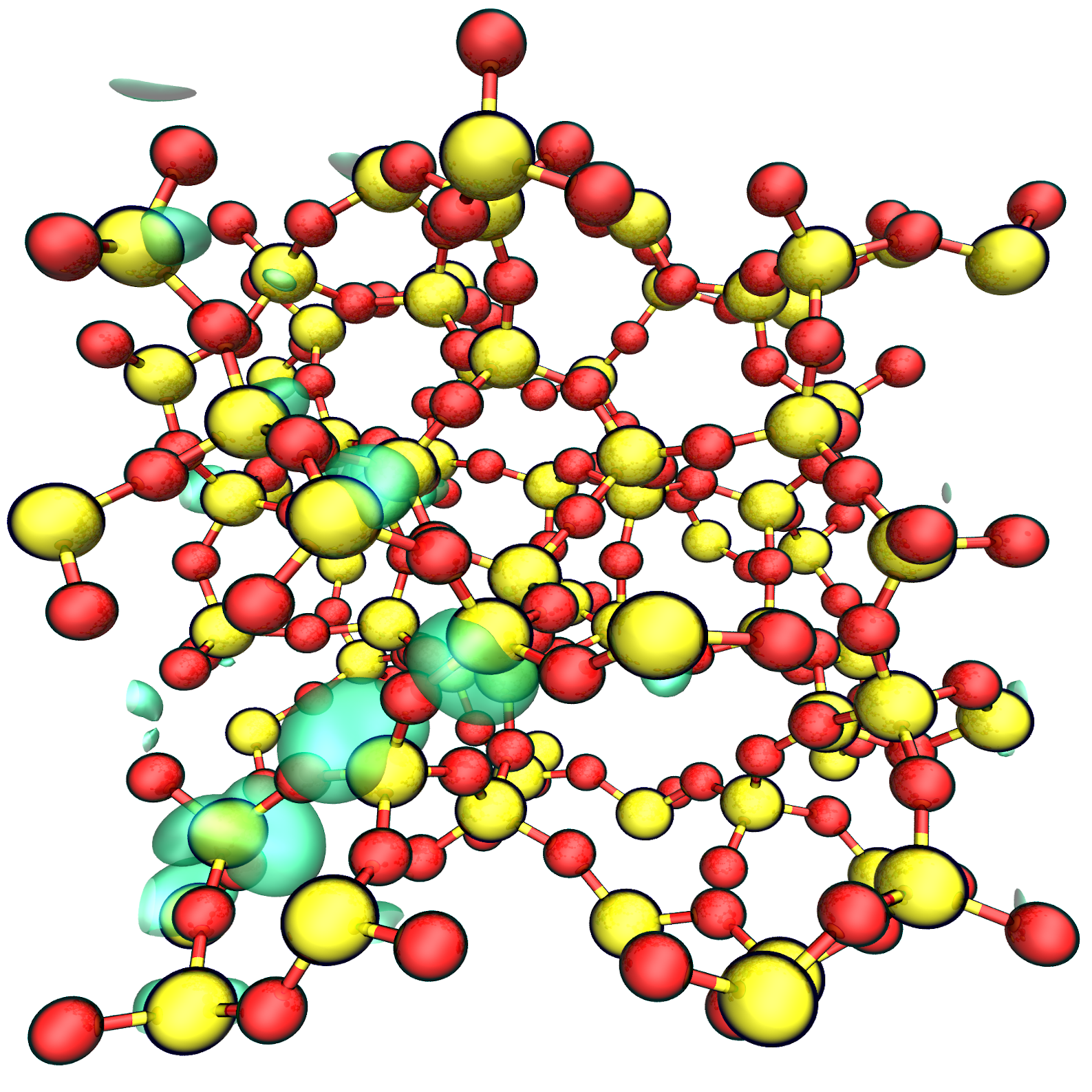
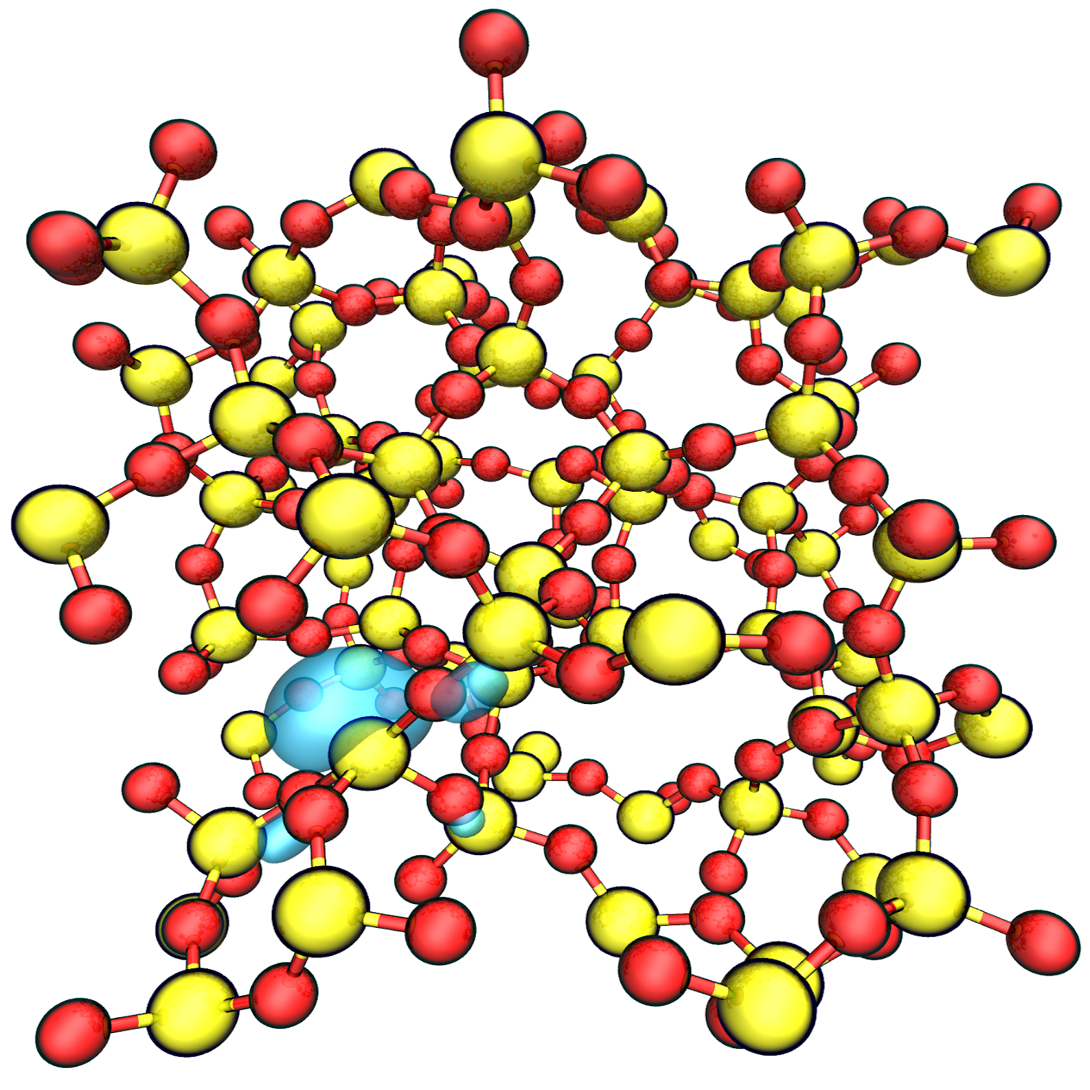
Figure 3.2: Ball-and-stick model of the a-SiO2 network with Si atoms (yellow) and oxygen atoms (red). An intrinsic electron trap is shown with a partly localized lowest unoccupied molecular orbital (LUMO) at an elongated O-Si-O bond (left). Upon electron capture, the wavefunction collapses onto the bond, which undergoes structural relaxation and further opens up the bond angle to reach values close to 180°, as can be seen from the intrinsic electron trap in its negative charge state, which is characterized by its highest occupied orbital (HOMO) (right).
Another defect candidate for electron capture in bulk a-SiO2 is the intrinsic electron trap, or polaron [177], shown in Figure 3.2. It stems from an intrinsic site in
the SiO2 network at which an electron may spontaneously localize at elongated O-Si-O bonds with bond angles  . The large density of these precursor sites of NT = 5 × 10¹⁹/cm3 estimated from their formation probability and their calculated thermodynamic trap level at ET = 2.8 eV below the
SiO2 conduction band edge make the defect a suitable candidate for electron trapping [177, CSC8]. Experimentally, the intrinsic electron trap is often linked to photon-stimulated electron tunneling measurements of shallow electron
traps [178], in which a large defect density of 1 × 10¹³/(cm2 eV) is extracted with an ET of 0.1 eV
below the conduction band edge of 4H-SiC in SiC/SiO2 MOS devices. It should be noted that a similar precursor site was calculated with DFT also for other binary oxides, i.e. ZrO2 and
HfO2 [179]. Within this work, the intrinsic electron trap is linked with TAT currents measured in SiC/SiO2 MOSCAPs.
Therefore, the calculations of El-Sayed et. al [177] are extended to observe statistical relevant parameter distributions of the thermodynamic
defect level and relaxation energies. Additionally, the same class of intrinsic traps can be linked to tunneling currents in ZrO2 based MIM capacitors within the NMP modeling framework Comphy, as will be discussed
in Chapter 5.
. The large density of these precursor sites of NT = 5 × 10¹⁹/cm3 estimated from their formation probability and their calculated thermodynamic trap level at ET = 2.8 eV below the
SiO2 conduction band edge make the defect a suitable candidate for electron trapping [177, CSC8]. Experimentally, the intrinsic electron trap is often linked to photon-stimulated electron tunneling measurements of shallow electron
traps [178], in which a large defect density of 1 × 10¹³/(cm2 eV) is extracted with an ET of 0.1 eV
below the conduction band edge of 4H-SiC in SiC/SiO2 MOS devices. It should be noted that a similar precursor site was calculated with DFT also for other binary oxides, i.e. ZrO2 and
HfO2 [179]. Within this work, the intrinsic electron trap is linked with TAT currents measured in SiC/SiO2 MOSCAPs.
Therefore, the calculations of El-Sayed et. al [177] are extended to observe statistical relevant parameter distributions of the thermodynamic
defect level and relaxation energies. Additionally, the same class of intrinsic traps can be linked to tunneling currents in ZrO2 based MIM capacitors within the NMP modeling framework Comphy, as will be discussed
in Chapter 5.