

Modeling of Defect Related Reliability Phenomena
in SiC Power-MOSFETs
Chapter 1 Introduction
The 2021 Intergovernmental Panel on Climate Change (IPCC) [1] report clearly states the urgent necessity to achieve a climate-neutral energy budget within the next decades. Hence, the ever-growing market of renewable energy production will further gain importance in the near future. Not only solutions for a carbon-free energy production but also approaches for a more efficient grid transport and therefore power conversion is among the highest priorities to meet the requirements of climate-neutrality with at the same time increasing power consumption. Electrical power conversion primarily requires a transformation of the voltage level and frequency, which is achieved by time-division of the input signal and transferring the energy into passive elements, e.g. an inductive coil on the output side. This signal partitioning requires an electrical switch, which is commonly realized by a Metal Oxide Semiconductor Field-Effect Transistor (MOSFET) or an Insulated Gate Bipolar Transistor (IGBT). Despite the significant improvements of the conversion efficiency that have been achieved in such devices based on silicon substrates, inevitable limits in the reduction of static and dynamic switching losses, as a consequence of the material properties of Si, have to be faced. These limits have been identified decades ago [2] and alternative substrate materials have attracted the attention of scientists and industry. These are so called wide-band gap semiconductors such as silicon carbide (SiC) and gallium nitride (GaN), that exhibit superior properties for power electronics to improve the conversion efficiency, have already made their way as substrate material into commercially available devices. Moreover, “exotic" substrate materials such as gallium oxide (Ga2O3) or diamond (C) promise further improvement in terms of power conversion efficiency and may fully replace Si-based power switches in the near future.

Figure 1.1: Electrical energy production (left) has more than doubled in the last 30 years, while renewable sources have increased their share of total energy production (data taken from [3]). Thus, advanced electronic systems become increasingly important. SiC MOSFETs when used as switches for power conversion circuits offer higher conversion efficiency (right), as a lower static on resistance can be achieved for a given voltage class, as shown for the third generation SiC DMOS technology of Cree Inc. [4] and for other SiC-DMOS and trench design SiC-MOSFETs (reproduced from [5]).
1.1 MOSFETs in Power Conversion Applications
The growing importance of renewable energy in total power consumption, as shown in the left panel of Figure 1.1, requires high efficiency for converting the voltage and frequencies at the generation and/or consumer site, as for instance at locally installed photo voltaic (PV) panels, to those required for the power grid. The task of finding the most suitable material for power conversion switches depends on many aspects of the application (e.g., voltage/power class, switching frequency) and eventually is limited by production costs, i.e. the economical feasibility of the production line that is used for the desired substrate material. Therefore, various materials and their impact on device properties have been studied in the past decades. A selection of the most important properties for power devices in general and those of SiC in particular are presented in the upcoming sections.
1.1.1 Materials
The natural limit of the minimum static on-state losses of a power switch built from a semiconductor material is defined by the relation of the blocking voltage  , that it is able to withstand, while at the same time sustaining a minimum (ideal) specific on-state resistance
![(1.1) \{begin}{align} R_\mathrm {on,sp} = \frac {4V_\mathrm {B}^2}{\varepsilon _s \mu _n E_C^3} \ignore {\left [ \si {\ohm \square \meter } \right ]}. \label {equ:ron} \{end}{align}](draftv0-images/image-5.svg)
A comparison of the natural limits for Si and SiC substrates together with already available SiC MOSFET technologies that exceed the Si limit is presented in Figure 1.1. By considering Baliga’s figure of merit [6]

which relies on the material parameters electrical permittivity  , the electron mobility
  and the critical field strength
  , the static power handling capabilities of an ideal device employing different substrate materials can be compared. Additional to the static losses, in a switching mode device with area
  the dynamic losses for a switching frequency
  at gate bias VG are added to the total conversion losses [2]

with the specific input capacitance  . With these quantities Baliga defined a high frequency operating device figure of merit, termed Baligas high frequency figure of merit (BHFFOM), by [2]

Johnson earlier formulated a FOM for the fundamental trade-off between a transition frequency within a channel length  and for a carrier saturation velocity
  with
with  = /
= /  and the power handling capability defined by the breakdown voltage across the channel
  as [7]

Besides the electrical material properties, heat management plays an important role in order to operate the power switch in a feasible temperature regime. Therefore, Keyes defined a figure of merit as [8]

with the specific thermal conductivity  and the speed of light
  to compare the heat dissipation limitations of the substrate material of power devices. Shenai et. al later proposed different thermal figures of merit depending on the heat dissipation coupling of the power
device, rather than just taking bulk properties into account [9].
to compare the heat dissipation limitations of the substrate material of power devices. Shenai et. al later proposed different thermal figures of merit depending on the heat dissipation coupling of the power
device, rather than just taking bulk properties into account [9].
|
Par. |
Si |
GaAs |
SiC |
GaN |
|
C (diamond) |
Unit |
|
|
11.7 |
12.9 |
9.76 |
8.9 |
10 |
5.7 |
1 |
|
EG |
1.12 |
1.42 |
3.26 |
3.39 |
4.85 |
5.5 |
eV |
|
|
0.3 |
0.4 |
1 |
4 |
8 |
10 |
MV/cm |
|
|
1400 |
8500 |
900 |
1000 |
300 |
2000 |
V/(cm s) |
|
|
1.5 |
0.55 |
3.7 |
2.1 |
0.2 |
6 |
W/(cm K) |


Table 1.1: Comparison of relevant parameters for substrate materials considered in power conversion devices, also shown in Figure 1.2 (right). Si-based power MOSFETs are still widely manufactured, while SiC and GaN based devices steadily increase their market share in their respective voltage classes. Data taken from [10, 11].
While Keys, Baligas, Johnsons and Shenais figures of merit mainly compare the bulk material properties of the substrate materials, Kim [12] tried
to take the impact of the output capacitance in a conversion circuit with a certain input voltage into account to define a new high frequency figure of merit (NHFFOM) by extending the approach of Baliga [2]. Moreover, Huang [13] defined a figure of merit (HDFOM) for
comparing unipolar switching devices based on the product of  and
and  , two quantities that can be obtained from measurements, assuming that the switching losses are dominated by the gate drain charge . In the same work, also the Huang chip area FOM (HCAFOM) is defined as HCAFOM =
  , whereby a higher FOM stands for less chip area necessary to sustain the same critical fields when conducting the same current density.

Figure 1.2: Figure of merits (left) and material properties (right) of different wide-band gap materials are compared. SiC and GaN as substrate materials offer advantages for applications in medium to high
voltage and high frequency classes, respectively, and both have already been introduced in commercial devices. While novel materials such as  -Ga
-Ga  O
O  show record breaking FOMs, material processing is hindering their introduction in commercial devices, an aspect that is not taken into account by most FOMs. Note that for the spider diagram representation the FOMs
and material properties have been normalized to the maximum value of each quantity (multiplied by a constant factor).
show record breaking FOMs, material processing is hindering their introduction in commercial devices, an aspect that is not taken into account by most FOMs. Note that for the spider diagram representation the FOMs
and material properties have been normalized to the maximum value of each quantity (multiplied by a constant factor).
Most of the FOMs purely consider bulk material properties, as listed in Table 1.1 for mature conventional (Si, GaAs) and wide band-gap (SiC, GaN) as well as more
exotic semiconductor materials (C, -Ga O ), and do not take into account process-ability and properties arising from their compatibility to potential insulators. Apparently, SiC does not provide record breaking FOMs and also the bulk material properties are not
exceeding those of e.g. GaN, except for heat conductivity, as shown in Figure 1.2. However, its ability to grow native SiO2 and the availability of high quality
substrates together with mature device processing techniques at reasonable cost outperforms GaN. Also, potential future candidates such as diamond within the medium to high blocking voltage class are far from large scale wafer
level production at this point in time. For instance, -Ga O with its wider bandgap and higher critical field strength promises even better breakdown voltage to on-resistance ratio compared to both GaN and SiC. Therefore, it has been suggested as a suitable substrate material
candidate for power devices within recent research works. However, p-doping of the material is particularly challenging due to the band-structure of -Ga O and has not been demonstrated yet [10]. With the largest bandgap and a high electron
mobility as well as superior thermal conductivity, diamond is well suited for harsh conditions such as high temperatures and blocking voltages. However, the high chemical stability of the material leading to these properties poses
severe challenges for device processing.
1.1.2 From MOSFETs to SiC Power Switches
A key step in the development of conventional MOSFETs has been the continuous improvement of the quality of the interface between the channel substrate material and the insulating layer. The electrically active “interface states" forming at the semiconductor-oxide transition region were the main reason that it took more than another three decades from Lilienfeld’s discovery of the field effect [14] until the first working MOSFET was demonstrated [15]. Thus, bipolar junction transistors (BJT) were the first to be used for logic circuits. However, with the introduction of annealing process steps MOSFETs outperformed BJTs and stand today at the heart of almost every electronic application. The basic working principle of a MOSFET is to modulate the conductivity of a channel, i.e. the density of free minority charge carriers in a thin layer situated in between two contact regions with opposing doping concentration compared to the channel. These are termed source and drain contacts and the modulating terminal is known as gate contact. The “set-in" gate bias point for forming this inversion layer, which opens a percolation path between the source and drain terminals, is defined as the threshold voltage Vth. Interface states and defects within the oxide in the vicinity of the channel, often referred to as near-interface traps (NITs) or border states, severely distort the device electrostatics and can lead to a drift of Vth when charged. By passivation of the Si surface and the interface to its stable native oxide SiO2, stable device operation can be achieved which has led to the success of integrated Si/SiO2 Complementary Metal Oxide Semiconductor (CMOS) processors.
An analogous development can be observed when looking at the history of the SiC MOSFET. Once SiC as bulk substrate material has been available in adequate quality for utilization in semiconductor devices in the 1990s [16, 17, 18], bipolar diodes were available soon afterwards in 2001 [19]. However, it took almost another decade until the first commercially available SiC MOSFETs entered the semiconductor device market in 2010 [20]. Since then, SiC MOSFETs have gained significant market share in the sector for devices with 0.9 kV to 15 kV blocking voltage [4]. An important milestone for the sucess of Si-based MOSFETS has been the improvement of the Si/SiO2 interface. Therefore, the interface properties have been studied over decades to optimize the interface carrier mobility and the threshold voltage stability by reducing the amount of electrically active defects, with e.g. forming gas anneals, in the vicinity of the channel. Such anneals have not shown to reduce the density of traps for SiC based MOSFETs with SiO2 used as an insulator. Thus, efforts to reduce the defect densities have just recently been successful by improving the annealing process in nitrogen enriched ambient after oxide deposition. Even though this led to a significant reduction of the SiC/SiO2 interface defect densities, it is still the determining factor for power loss improvement, as scattering at the remaining interface and border states reduces the carrier mobility and thereby dominates Ron. Thus, to date large efforts towards a more detailed understanding of the electrical properties of the defects at the interface region, such as presented within this work, have been made. Before discussing the reliability threats caused by defects in more detail, the bulk SiC properties and MOSFET device fabrication will be outlined in the next two sections.
1.1.3 Silicon Carbide Material Properties
Carborundum, as silicon carbide is termed natively, is stoichiometrically composed by an equal number of Si and C atoms. Among the various polytypes in which SiC can crystallize [21], the four layered hexagonal (4H-SiC) polytype has been instituted in commercially available SiC power-switches. In the notation of Ramsdell, the polytype is denoted by the number of Si-C bilayers within the unit cell, shown in Figure 1.3, and the crystal system (H for hexagonal), hence 4H-SiC. Due to its superior mobility and breakdown values, the 4H- has ousted the 6H-SiC polytype as substrate material for power MOSFETs [22]. Therefore, this polytype is referred to throughout this work, unless otherwise noted.
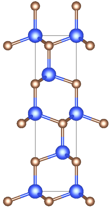

Figure 1.3: Unit cell of 4H-SiC (left) with equal number of C (brown) and Si (blue) atoms, reproduced from [23,
24], is shown together with technologically relevant crystal planes in SiC MOSFETs and translation vectors (right). Note the Si-face (0001)-
plane is typically the terminating surface in lateral and the a-face (11  0)-plane in vertical MOSFETs.
The stacking sequence of SiC is shown together with crystal planes and translation vectors, which are technologically relevant for modern MOSFET architectures, in Figure 1.3. A 1/2 hexagonality can be seen for the 4H polytype, with half of the bilayers crystallyzing on hexagonal sites within the unit cell. The two lattice constants for the 4H
crystal structure are given by  = 3.0789 Å,
  = 10.082 Å. The covalent Si-C bond has a binding energy of
  , with a weak ionicity, as the valence electrons localize closer to the carbon atom (c.f. electro negativity: C: 2.5, Si: 1.8).
The electronic band structure of 4H-SiC exhibits an indirect bandgap of 3.26 eV [25] at
room temperature from the  (top valence band) to
  (minimum conduction band) point and features
  = 3 conduction band minima within the first Brillouin-zone. The temperature dependence of the bandgap due to thermal expansion can be described by the Varshni model [26]

with  = 3.5 × 10⁻⁴ eV/K, = 1.1 × 10³ K and
  = 3.285 eV [27, 28].
Due to the hexagonal crystal structure, the effective masses in the perpendicular and parallel planes to the c-axis exhibit a strong anisotropy. The parallel electron effective mass measured by cyclotron resonance is given by  = 0.31
  , while the perpendicular mass is given by
  = 0.48 . Hole effective masses were extracted with = 1.75 and
  = 0.66 [29, 30].
By applying the concept of density of states (DOS) effective masses for electrons and holes
= 0.66 [29, 30].
By applying the concept of density of states (DOS) effective masses for electrons and holes  , the effective DOS in conduction and valence band is given by [31]

As the calculated effective DOS is not exactly proportional to  , the effective masses need to be modeled as temperature dependent too. The thermal DOS effective masses calculated by using the
  method [32] have been fitted with polynomials [33]

for the application in device simulations.
Moreover, the carrier mobilities show anisotropic values parallel and perpendicular to the c-axis, with about 20 % higher mobilities in the parallel direction. Note that at room temperature ionized impurity scattering is the limiting mechanism for mobility in bulk SiC and can be described by the Caughey-Thomas equation [34]

with  ,
,  ,
,  ,
,  and the doping ratio exponents
  and
and  . Note that these values are given for high purity SiC grown by epitaxy and will be decreased in bulk SiC grown by sublimation due to scattering at the increased numbers of point and stacking defects. At higher
temperatures the acoustic phonon and inter-valley scattering become the dominant scattering mechanisms and the doping concentration dependence of the mobilities decreases.
. Note that these values are given for high purity SiC grown by epitaxy and will be decreased in bulk SiC grown by sublimation due to scattering at the increased numbers of point and stacking defects. At higher
temperatures the acoustic phonon and inter-valley scattering become the dominant scattering mechanisms and the doping concentration dependence of the mobilities decreases.
1.1.4 Fabrication and Properties of SiC MOSFETs
A first step for the successful fabrication of commercially available SiC MOSFETs was the production of largely defect free SiC substrate wafers. A solution growth of large area bulk SiC ingots, which is the standard technique used
for Si wafer production, imposes many challenges such as low solubility of C even at large temperature. Additionally, a high pressure (e.g. 100 bar) under inert Ar conditions is required and the reaction of the melt with the
graphite crucible can not fully be omitted, which requires the development of other wafer production methods. Seeded-sublimation growth has been established to grow bulk ingots making reasonable quality SiC wafers of up to
150 mm diameter available. In this boule growth method, sintered poly-crystalline SiC is typically sublimed within a graphite crucible. The sublimed source species then move towards a seed crystal of the intended
poly-type with high crystalline quality, due to a defined temperature gradient within the crucible. A surface reaction and crystallization step at the lower temperature seed crystal leads to the desired controlled poly-type crystal
growth. The crucible is thereby heated to  2300 °C to 2400 °C, while the seed temperature is about 100 °C lower. Exact process control is required during crystal growth as defect formation energies for stacking, dislocation,
and point defects are relatively low for the desired 4H-SiC polytype. Inert gas is introduced during the crystal growth to minimize impurity incorporation and by consideration of reaction kinetics and thermodynamics,
performance-limiting defects in the bulk SiC have been significantly reduced in the past [35, 36]. However, to achieve the required crystal quality, i.e. defect free poly-type preserved grown SiC with controlled doping and thickness, homoepitaxy
has become an essential growth technique for the production of SiC devices that can compete with their Si-based counterparts. The lightly doped drift layer on top of the heavy doped substrate used as the drain contact is grown by
chemical vapor deposition (CVD) technique employing silan (SiH
2300 °C to 2400 °C, while the seed temperature is about 100 °C lower. Exact process control is required during crystal growth as defect formation energies for stacking, dislocation,
and point defects are relatively low for the desired 4H-SiC polytype. Inert gas is introduced during the crystal growth to minimize impurity incorporation and by consideration of reaction kinetics and thermodynamics,
performance-limiting defects in the bulk SiC have been significantly reduced in the past [35, 36]. However, to achieve the required crystal quality, i.e. defect free poly-type preserved grown SiC with controlled doping and thickness, homoepitaxy
has become an essential growth technique for the production of SiC devices that can compete with their Si-based counterparts. The lightly doped drift layer on top of the heavy doped substrate used as the drain contact is grown by
chemical vapor deposition (CVD) technique employing silan (SiH  ) and propan (C
  H
H  ) or ethylene (C
  H ) as precursors. The employment of a 4° off-axis angle on the substrate allows to perfectly rebuild the required stacking sequences of the hexagonal polytypes [37, 38].
With high quality substrates available, the most important process steps for the production of MOSFETs on SiC substrates are outlined further. High energy ion-implantation is used to form doping regions of n- and p-type
conductivity, as a diffusion process is not applicable due to the significantly smaller diffusion constants of dopands within SiC [39]
compared to Si. After the implantation, the damaged rough SiC surface is typically carbonized forming a carbon cap for subsequent mass production steps [40]. High-temperature post-implantation anneals are required for higher dose implantation for successful lattice recovery and doping activation.
Aluminum is typically used as p-type dopand, while Phosphorus or Nitrogen are used for n-type doping. Al incorporates into the SiC lattice either on a hexagonal or cubic Si site with ionization energy  200 meV, which results in only a fraction of dopands ionized even at room temperature. With
  60 meV for both, P substituting a Si on a cubic site and N for C on a hexagonal site, these dopands can be considered ionized at room temperature at low concentration (i.e.
  1 × 10¹⁶/cm3). The fraction of ionized dopands is given by

with the degeneracy factors  determined by the band-structure of the host material and the Fermi level
  .
.  denote the maximum electrically active doping concentration, i.e. the concentration of the fully ionized dopands.
A major advantage above other compounds, e.g. GaN, is that SiC can be thermally oxidized to form a high quality oxide, i.e. SiO2, for MOS devices and a passivation layer for SiC surfaces. The dry oxidation process is described by the reaction

A similar amount of bulk SiC as for Si, namely 46 %, is consumed for the SiO2 growth, i.e. 10 nm SiO2 are grown by consuming 4.6 nm SiC. It has to be mentioned that a dry
thermal oxidation of SiC is time consuming and it takes more than 6 h to grow a 50 nm thick SiO2 layer, as typically required for power switches, on the (0001)-terminated face at  = 1150 °C [41]. The oxidation process is strongly anisotropic and about ten times
faster on the a-face surface at the same when compared to the oxidation of Si-face surfaces. This implies also strong oxide thickness variation along a trench MOSFET, i.e. smallest thickness on top and bottom of the trench and thicker at the sidewalls. Besides
the strong anisotropy in growing rate at different surfaces, dry thermal growth leads to increased carbon incorporation at the interface as O in-diffusion and CO out-diffusion are reported to be the rate limiting mechanisms in thick SiO2 layers [41]. Oxide growth via atomic layer deposition (ALD) can resolve the anisotropy problem and additionally increases the interface stability [42]. However, it is an unfeasible process step for economic power device processing due to the long duration required to grow thick oxides. Therefore,
the oxide deposition via a low-pressure chemical vapor deposition (LPCVD) employing tetra-ethyl-ortho-silicat (TEOS) as a precursor [43, 44] offers an alternative with the additional benefit of a reduced thermal budget at the gate stack.
= 1150 °C [41]. The oxidation process is strongly anisotropic and about ten times
faster on the a-face surface at the same when compared to the oxidation of Si-face surfaces. This implies also strong oxide thickness variation along a trench MOSFET, i.e. smallest thickness on top and bottom of the trench and thicker at the sidewalls. Besides
the strong anisotropy in growing rate at different surfaces, dry thermal growth leads to increased carbon incorporation at the interface as O in-diffusion and CO out-diffusion are reported to be the rate limiting mechanisms in thick SiO2 layers [41]. Oxide growth via atomic layer deposition (ALD) can resolve the anisotropy problem and additionally increases the interface stability [42]. However, it is an unfeasible process step for economic power device processing due to the long duration required to grow thick oxides. Therefore,
the oxide deposition via a low-pressure chemical vapor deposition (LPCVD) employing tetra-ethyl-ortho-silicat (TEOS) as a precursor [43, 44] offers an alternative with the additional benefit of a reduced thermal budget at the gate stack.
However, as is the case for silicon MOSFETs, the interfacial strain and stoichiometric disorder at the transition region to the bulk amorphous oxide leads to electrically active unsaturated dangling bonds, e.g.
Pb,0-centers for Si/SiO2. In Si-MOSFETs, these defects are passivated by a forming gas (H ) ambient annealing process step, thereby reducing the number of interface states from Dit  1 × 10¹³/(cm2 eV) [45] to Dit 1 × 10¹⁰/(cm2 eV) [46]. Unlike for Si surfaces and
the Si/SiO2 interface, hydrogen passivation has not shown to significantly reduce the interface state density for SiC/SiO2 MOS structures [47]. Only the implementation of a Post Oxidation Annealing (POA) or Post Deposition Annealing (PDA) step in nitrogen enriched ambient
has lead to a sufficient reduction of interface states at the SiC/SiO2 transition region and enough stability for surface passivation [20]. Typically, nitridation of the interface can be achieved in ambients containing nitrous oxide NO , nitric oxide NO or ammonia NH3 at temperatures of above 1300 K. However, even with years of POA and PDA optimization, the Dit 1 × 10¹¹/(cm2 eV) observed in SiC MOSFETs is still two orders of magnitude higher than in Si-technologies.
1 × 10¹³/(cm2 eV) [45] to Dit 1 × 10¹⁰/(cm2 eV) [46]. Unlike for Si surfaces and
the Si/SiO2 interface, hydrogen passivation has not shown to significantly reduce the interface state density for SiC/SiO2 MOS structures [47]. Only the implementation of a Post Oxidation Annealing (POA) or Post Deposition Annealing (PDA) step in nitrogen enriched ambient
has lead to a sufficient reduction of interface states at the SiC/SiO2 transition region and enough stability for surface passivation [20]. Typically, nitridation of the interface can be achieved in ambients containing nitrous oxide NO , nitric oxide NO or ammonia NH3 at temperatures of above 1300 K. However, even with years of POA and PDA optimization, the Dit 1 × 10¹¹/(cm2 eV) observed in SiC MOSFETs is still two orders of magnitude higher than in Si-technologies.
The high interface state density also dominates the channel electron mobility due to electron scattering at these charged defects. In bulk 4H-SiC the dominant scattering mechanisms are acoustic and intervalley scattering for lightly
doped (  ) regions. For increased doping densities of
  , as approximately used for channel doping concentrations, neutral impurity and invervalley scattering dominate at room temperature and above, resulting in an electron mobility of about
  at room temperature, as extracted by Hall measurements and theoretical calculations [48].


Figure 1.4: ID (VG ) characteristics for lateral Si-face (0001) n-MOSFETs with L=8 µm, W=100 µm and  = 70 nm gate oxide with NO-POA for varying temperature in the range of 100 K to 600 K (left). The channel mobilities (top, right) are extracted by the method of Ghibaudo [49] and with the effective mobility equation [22].
The threshold voltage is extracted by a constant current method and the maximum
= 70 nm gate oxide with NO-POA for varying temperature in the range of 100 K to 600 K (left). The channel mobilities (top, right) are extracted by the method of Ghibaudo [49] and with the effective mobility equation [22].
The threshold voltage is extracted by a constant current method and the maximum  method (bottom, right).
This value decreases to about 50 cm2/(V s) at a temperature of 100 K. However, as shown in Figure 1.4, when extracting mobility
values from  (
(  ) characteristics at different temperatures for lateral (Si-face) MOSFETs, an opposing trend is observed, with increasing Ghibaudo mobilities [49] for higher at significantly smaller absolute values. This behavior can mainly be explained by reduced Coulomb scattering at higher , due to less interface charge trapped [50]. Also, a strong correlation of the reduced
mobility with large interface state densities has been extracted on different SiC surface termination planes at the interface to SiO2 [22]. Thus, it has been revealed that the a-face surface shows larger mobilities compared to the Si-face, due to reduced interface state densities close
to the SiC conduction band edge [51]. Therefore, UMOSFET (or trench) architectures with a vertical channel along the a-face crystal plane,
contrary to DMOSFETs with channel planes along the Si-face as shown in Figure 1.5, have been introduced by manufacturers recently.
) characteristics at different temperatures for lateral (Si-face) MOSFETs, an opposing trend is observed, with increasing Ghibaudo mobilities [49] for higher at significantly smaller absolute values. This behavior can mainly be explained by reduced Coulomb scattering at higher , due to less interface charge trapped [50]. Also, a strong correlation of the reduced
mobility with large interface state densities has been extracted on different SiC surface termination planes at the interface to SiO2 [22]. Thus, it has been revealed that the a-face surface shows larger mobilities compared to the Si-face, due to reduced interface state densities close
to the SiC conduction band edge [51]. Therefore, UMOSFET (or trench) architectures with a vertical channel along the a-face crystal plane,
contrary to DMOSFETs with channel planes along the Si-face as shown in Figure 1.5, have been introduced by manufacturers recently.


Figure 1.5: Sections of a DMOSFET (a) and an UMOSFET (b) are shown with cuts along the vertical symmetry axis of the devices. A tens of nm thick oxide is deposited on the trench sidewalls. The channel surface area along
the SiC (011 ) plane in the trench case and along the (0001) plane in the DMOSFET case are highlighted in red. While highest channel mobility values are reported along the vertical interface orientation, charge trapped at interface and
bulk-oxide defects, schematically indicated by yellow balls, severely reduce channel mobility compared to bulk values at both surfaces. In order to simplify the device representations, details such as passivation doping and correct
aspect ratios are spared out.
Additionally, channel counter doping by donor incorporation (for n-channel MOSFETs) has been studied extensively, with e.g. N, P, Sb and Ba incorporated in a thin layer at the SiC/SiO2 interface [52, 53]. The effect of these thin counter-doping layers is a electrostatic potential screening that leads to smaller field strengths required to build up the same inversion layer carrier density and also less surface scattering. In turn, higher low field channel mobilities can be observed, with diminishing effect at higher fields [52].