1 Introduction
Semiconductor devices were the key enabler for the arrival of the computer age, also known as the second industrial revolution. At the heart of the information and communication technologies, integrated circuits (ICs) - based on an ensemble of semiconductor devices - find applications in consumer electronics, automobiles, medical equipment, industrial devices, and many more. The dominant semiconductor for the majority of electronic devices has for a long time been silicon (Si). However, recently wide-bandgap semiconductors, particularly silicon carbide (SiC), attracted much attention because of many key benefits over other semiconductor materials in a large number of industrial and military applications [1, 2]. Although Si has been used for high-power, high-temperature, and high-frequency devices, significant performance improvements of Si devices can no longer be expected, because the devices have reached their performance limit introduced by the material’s inherent physical properties [3]. Thus, SiC power devices will set new standards in power savings for virtually everything that converts or uses electricity, from wind turbines and solar installations to industrial data centers, hybrid cars, and medical imaging systems, just to name a few. Apart from the significant progress achieved in the area of SiC-based electronics continued advancements in numerical simulations are necessary to enhance the design and optimization of SiC devices, which will further optimize the devices and reduce fabrication costs. The development of novel electronic devices thus requires accurate one- (1D), two- (2D), and three-dimensional (3D) modeling approaches to be able to predict physical phenomena during device fabrication and operation.
1.1 Silicon Carbide
Naturally occurring SiC, also known as moissanite, is extremely rare and can be found only in certain types of meteorite. It was found in 1983 as a small component of the Canyon Diablo meteorite in Arizona [4]. Because of the rarity of natural moissanite, most of SiC is synthetic. The simplest manufacturing process is to combine silica sand and carbon (C) in an Acheson graphite electric resistance furnace [5] at a high-temperature, between 1600°C and 2500°C. The material formed in the Acheson furnace varies in purity, according to its distance from the graphite resistor heat source. Pure SiC can be made by the Lely process, in which SiC powder is sublimated into high-temperature species of Si, C, silicon dicarbide (SiC2), and disilicon carbide (Si2C) in an argon gas ambient at 2500°C and finally redeposited into flake-like single crystals [6]. This method was extended as seeded sublimation technique in the late 1970s [7]. The latter method was further refined in the early 1990s [8] for producing large-diameter SiC boules. Various modifications of these techniques are now used at many laboratories worldwide. Bulk single crystals of SiC with diameters of >100 mm are fabricated today [9].
Among the wide-bandgap semiconductors, SiC is the only compound semiconductor which can be thermally oxidized in the form of silicon dioxide (SiO2), similarly to Si. Devices which can be fabricated on Si substrates, such as power metal-oxide-semiconductor field-effect transistors (MOSFET) and insulated-gate bipolar transistors (IGBT), can thus also be fabricated on SiC substrates. Therefore, SiC is considered to be a post Si power device material, as SiC offers superior physical properties over Si, such as wide-bandgap, high electrical breakdown voltage, and high thermal conductivity [10, 11]. However, in order to take advantage of these superior properties of SiC, many challenges on the material level must be better understood and eventually overcome, particularly concerning crystal structure, substrate orientation, bond formation, dopant activation, and ionization [12].
1.1.1 Crystallography
SiC exists in more than 250 crystal structures, known as crystalline forms, which are called polytypes [13]. They are variations of the same chemical compound, which are identical in two dimensions and differ in the third. Thus, the polytypes can be viewed as layers stacked in a certain sequence [14]. Each SiC bilayer can be oriented into only three possible positions with respect to the lattice, while the tetrahedral bonding is maintained. These three layers are arbitrarily denoted A, B, and C. The most common polytypes of SiC presently being developed for electronics are the cubic 3C-SiC, the hexagonal 4H-SiC and 6H-SiC, and the rhombohedral 15R-SiC. 3C-SiC is the only form of SiC with a cubic crystal lattice structure which is similar to Si. The prefix number, e.g., 3 in 3C-SiC, refers to the number of layers needed for periodicity, i.e., the stacking sequence ABC. 4H-SiC consists of an equal number of cubic and hexagonal bonds with a stacking sequences of ABAC, while 6H-SiC is composed of two-thirds cubic bonds and one-third hexagonal bonds with a stacking sequence of ABCACB. The overall symmetry is hexagonal for both polytypes, despite the cubic bonds which are present in each. Cubic lattice sites are typically denoted as k and hexagonal sites as h. Similarly, 15R-SiC is a rhombohedral crystal structure composed of three-fifth cubic bonds and two-fifth hexagonal bonds. The stacking sequences among common SiC polytypes are summarized in Table 1.1.
Changing the stacking sequence of SiC has an impact on the mechanical material properties [15], particularly on lattice constants, i.e., basic cell dimensions. The lattice height b of 6H-SiC is approximately 1.5 times higher than of 4H-SiC. However, the lattice width a is almost identical for both hexagonal polytypes. In contrary, the basic cube dimension of 3C-SiC is higher than the hexagon width of 4H- and 6H-SiC, while the density of all three polytypes remains equal. The common SiC polytypes have, compared to Si, gallium nitride (GaN), and gallium arsenide (GaAs), approximately a five times higher thermal conductivity and an approximately two times higher melting point1. The mechanical properties of 3C-SiC, 4H-SiC, 6H-SiC, Si, and GaAs are summarized in Table 1.2.
Table 1.1: Stacking sequences of common SiC polytypes. k and h refer to cubic and hexagonal lattice sites, respectively.
| Polytype | Stacking Sequence | No. k | No. h |
| 3C | ABC | 1 | 0 |
| 4H | ABAC | 1 | 1 |
| 6H | ABCACB | 2 | 1 |
| 15R | ABCACBCABACABCB | 3 | 2 |
Table 1.2: Mechanical material properties of common SiC polytypes and other common semiconductors. a and b are the width and the height of the crystal unit cell, respectively, ρ is the density of the crystal unit cell, λ is the thermal conductivity, and Tmelt is the melting point.
| Property | 3C-SiC | 4H-SiC | 6H-SiC | Si | GaAs |
| a [Å] | 4.359 | 3.073 | 3.081 | 5.43 | 5.65 |
| b [Å] | 4.359 | 10.05 | 15.12 | 5.43 | 5.65 |
| ρ [gm/cm3] | 3.2 | 3.2 | 3.2 | 2.3 | 5.3 |
| λ [W/cmK] | 5 | 5 | 5 | 1.5 | 0.5 |
| Tmelt [°C] | 2830 | 2830 | 2830 | 1420 | 1240 |
Today, only 4H- and 6H-SiC polytypes are available commercially as substrate materials. Among the hexagonal polytypes, 4H-SiC is the most promising polytype being already implemented in various applications, such as high-voltage MOSFETs [16, 17], and is thus the focus of this thesis. 4H-SiC has the stacking sequence ABAC. The layer structure of 4H-SiC is shown in Figure 1.1.
The typically used notation system for crystallographic planes, also known as faces, are Miller indices [18]. For the cubic crystal three Miller indices, h, k, and l, are used to describe directions and planes in the crystal. These are integers with the same ratio as the reciprocals of the intercepts with x-, y-, and z-axis, respectively. h, k, and l denote the family of planes orthogonal to hb1 + kb2 + lb3, where b1, b2, and b3 are the reciprocal lattice vectors. Correspondingly, the three primitive lattice vectors which define the unit cell are a1, a2, and a3.
For hexagonal structures, however, four Miller indices are commonly used, denoted h, k, i, and l, which must obey the constraint h + k + i = 0. Correspondingly, four primitive lattice vectors a1, a2, a3, and c are defined for the hexagonal unit cell. The sum of the reciprocal intercepts with a1, a2, and a3 is zero. The angle γ between the a-vectors is 120°, whereas the c-vector is perpendicular to the plane of the a-vectors. A representative selection of basic planes as examples of determining Miller indices is shown in Figure 1.2. In the case of 4H-SiC the four commonly investigated crystallographic faces are the (\(0001\)) Si-, (\(000\bar {1}\)) C-, (\(1\bar {1}00\)) m-, and (\(11\bar {2}0\)) a-face, shown in Figure 1.3. Despite the fact that all SiC polytypes chemically consist of 50% carbon atoms bonded with covalent (i.e., molecular) bonds to 50% Si atoms, each SiC polytype has its own distinct set of physical properties [19].
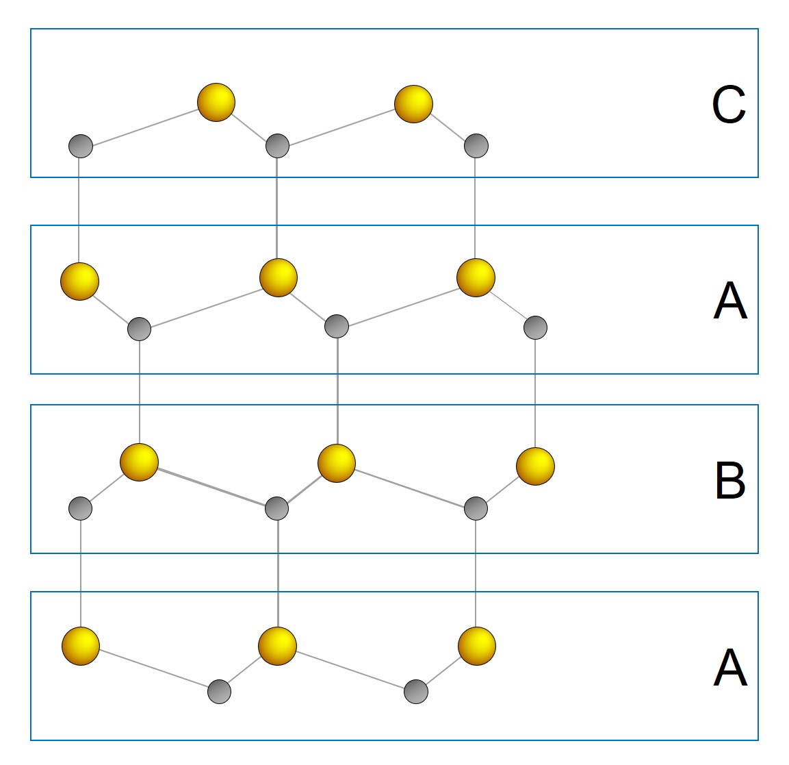
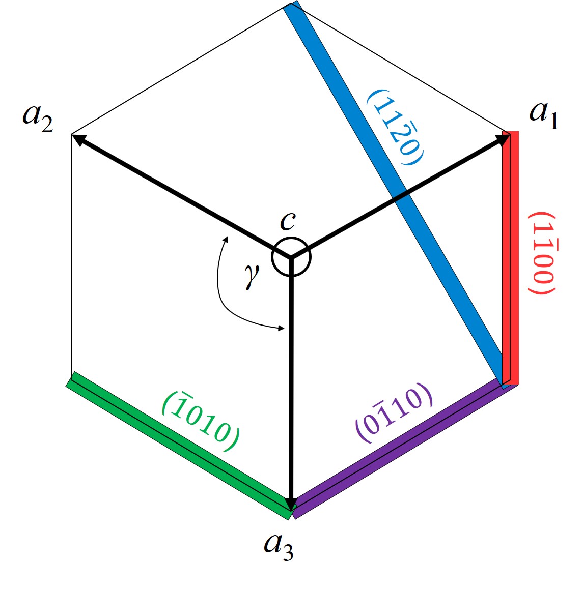
Figure 1.2: Examples of Miller indices for a hexagonal crystal structure, showing a representative selection of basic planes: (\(\bar {1}010\)) (green), (\(0\bar {1}10\)) (violet), (\(1\bar {1}00\)) (red), and (\(11\bar {2}0\)) (blue square). a1, a2, a3, and c are the primitive lattice vectors and γ=120° is the angle between the a-vectors. The vector c is perpendicular to the a-vectors and points into the drawing plane.
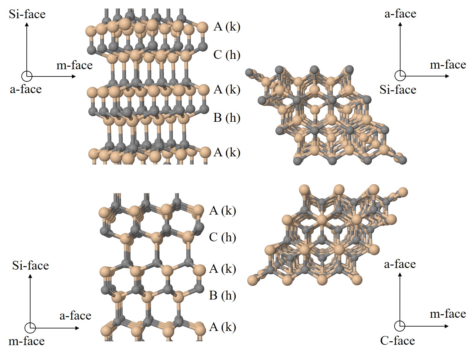
Figure 1.3: 3D schematic illustrations of various perspectives of a 4H-SiC polytype with the stacking sequence ABAC. The brown spheres represent Si atoms, the gray spheres C atoms, and the arrows show directions towards corresponding crystallographic faces. The Miller indices are: Si-face \((0001)\), C-face \((000\bar {1})\), m-face \((1\bar {1}00)\), and a-face \((11\bar {2}0)\). h and k stand for the hexagonal and cubic lattice sites, respectively.
1 The melting point refers to the temperature at which a solid changes its state to liquid at atmospheric pressure.
1.1.2 Physical Properties
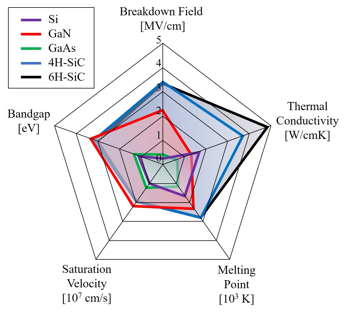
The properties of SiC make it the foremost semiconductor material for short wavelength optoelectronic, high-temperature, radiation resistant, high-power, and high-frequency electronic devices [20]. SiC-based devices can operate at high temperatures without suffering from intrinsic conduction effects, because of its wide-bandgap. SiC can withstand electric fields five to twenty times larger than Si or GaAs without undergoing avalanche breakdown [21]. This high breakdown electric field allows the devices to be closer together, providing high device packing density for integrated circuits. SiC is in addition an excellent thermal conductor, e.g., at room temperature (300 K) it has a three to thirteen times higher thermal conductivity than Si [22]. The high thermal conductivity enables SiC-based devices to operate at extremely high power levels whilst still being able to dissipate the large amounts of generated excess heat. SiC devices can operate at high frequencies, such as radio and microwave frequency ranges, due to the larger saturated electron drift velocity, which is two to two-and-a-half times larger than that of Si [23]. Comparisons of the bandgap, breakdown field, thermal conductivity, melting point, and saturation velocity of Si, GaN, GaAs, 4H-SiC, and 6H-SiC are shown in Figure 1.4.
The arrangement of next neighbors in the lattice is the same for all SiC polytypes, but crystallographic nonequivalent lattice sites exist in different polytypes. Thus, electronic properties, such as effective mass, carrier mobility, and bandgap, vary between different SiC stacking sequences and crystal orientations. Different polytypes have profound effects on the material properties, for example, the bandgap changes from 3.2 eV (4H-SiC) to 2.4 eV (3C-SiC). Some of the SiC properties are anisotropic, i.e., direction-dependent with respect to the crystal orientation. One example is the electron mobility which is in the case of 6H-SiC 60 cm2/Vs parallel to the c-axis and 400 cm2/Vs perpendicular to the c-axis. The low anisotropy of the electron mobility in 4H-SiC is one of the primary reasons for the emerging popularity of 4H-SiC, compared to 6H-SiC which has an extremely high anisotropic electron mobility.
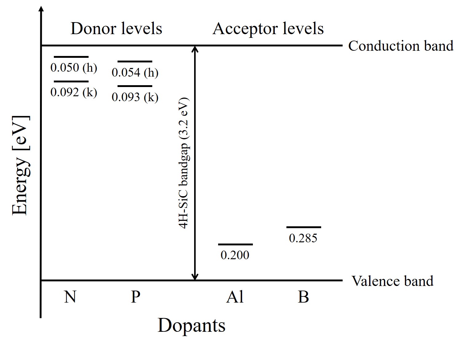
Dopants in SiC can be incorporated into energetically nonequivalent cubic (k) or quasi-hexagonal (h) lattice sites, as shown in Figure 1.5. Hall measurements have yielded two donor levels upon the occupancy site in 6H-SiC, i.e., the hexagonal site is 85 meV and the cubic site is 140 meV. In 4H-SiC the donor levels of nitrogen (N)-doped SiC are 50 meV and 92 meV for hexagonal and cubic sites, respectively. For phosphorus (P)-doped SiC the donor levels are 54 meV and 93 meV for hexagonal and cubit sites, respectively [10]. The fact that most dopant levels are deeper than those found comparably in Si explains the partial carrier freeze-out in SiC at room temperature, since the thermal energy is only ≈ 25.9 meV at 300 K. In contrast, for p-type aluminium (Al)-doped SiC, an average acceptor energy level in the range of 200 to 240 meV is found for all polytypes. Other p-type dopants such as boron (B) have deeper acceptor levels (≈ 300 meV), but are not commonly used.
The effective mass of an electron or a hole is usually stated in units of the rest mass of an electron m0 = 9.11 · 10-31 kg. In these units the effective mass of electrons or holes is commonly in the range from 0.01 to 10, but can be as high as 1000 for exotic heavy fermion materials [24]. The experimental and theoretical values of the longitudinal and transverse effective mass of electrons and holes in SiC are still diverging across the literature for various polytypes and directions [1]. However, typically used values for calculating carrier concentrations are based on Hall effect analyses: The effective mass of electrons at 300 K for 4H-SiC is 0.4 m0 [25] and for 6H-SiC 0.6 m0 [26]. The effective mass of holes at 300 K for 4H-SiC is 2.6 m0 and for 6H-SiC 2.8 m0. These differences clearly show that the effective mass of the electrons and holes are polytype-dependent.
All of the electrical properties of 4H- and 6H-SiC are summarized in Table 1.3. For comparison the properties of Si are shown as well. The major SiC polytypes exhibit advantages and disadvantages in basic material properties compared to Si. However, the main advantages of SiC over Si are particularly the thermal conductivity, the electrical breakdown strength, and the bandgap, which all together allow for higher temperature, frequency, and voltage operation of SiC-based devices.
Table 1.3: Comparison of electrical properties of common SiC polytypes, SiC anisotropy, and Si. Eg is the bandgap, εs the relative dielectric constant, EB the breakdown field, λ the thermal conductivity, ni the intrinsic carrier concentration, μn the electron mobility, μp the hole mobility, ED the ionization energy of donors, EA the ionization energy of acceptors, MC the number of equivalent minima in the conduction band, me* the effective mass of an electron, mh* the effective mass of a hole, and m0 = 9.11 · 1031 kg the electron rest mass. \(\parallel\) and \(\bot\) refer to parallel and perpendicular directions, respectively, and k and h refer to cubic and hexagonal lattice sites. μn and μp are measured at donor and acceptor concentration 1016 cm-3, EB at donor concentration 1017 cm-3, and me* and mh* at temperature 300 K [1, 10, 27, 28, 29, 30, 25, 26].
| Property | 4H-SiC | 6H-SiC | Si | |
| Eg [eV] | 3.2 | 3.0 | 1.12 | |
| εs | 9.7 | 9.66 | 11.9 | |
| EB [MV/cm] |
\(\parallel\) c-axis: 3.0 \(\bot\) c-axis: 1.0 |
\(\parallel\) c-axis: 3.2 \(\bot\) c-axis: 1.0 |
0.3 | |
| λ [W/cm K] | 3.7 | 4.9 | 1.31 | |
| ni [cm-3] | 5.0 · 10-9 | 1.6 · 10-6 | 9.65 · 109 | |
| μn [cm-2/Vs] |
\(\parallel\) c-axis: 900 \(\bot\) c-axis: 800 |
\(\parallel\) c-axis: 60 \(\bot\) c-axis: 400 |
1430 | |
| μp [cm-2/Vs] | 115 | 90 | 480 | |
| Donor: ED [meV] |
N: 50 (k), 92 (h) P: 54 (k), 93 (h) |
N: 85 (k), 140 (h) P: 80 (k), 110 (h) |
P: 45 As: 54 |
|
| Acceptor: EA [meV] |
Al: 200 B: 285 |
Al: 240 B: 300 |
Al: 67 B: 45 |
|
| MC | 3 | 6 | 6 | |
| me* | 0.4 m0 | 0.6 m0 | 0.2 m0 | |
| mh* | 2.6 m0 | 2.8 m0 | 0.4 m0 | |
1.1.3 Device Applications
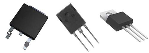
Several SiC semiconductor devices, utilized mostly in high-power applications [31, 32, 33], are commercially available, such as Schottky barrier diodes (SBDs), junction-gate field-effect transistors (JFETs), and MOSFETs, shown in Figure 1.6. The first commercial 1200 V JFETs were introduced in 2008, followed by the first commercial 1200 V MOSFETs in 2011. In the same timeframe some companies started implementing bare SiC Schottky diode chips into their power electronic modules. In fact, SiC SBDs are widely used in IGBT power modules and power factor correction circuits.
Power devices and electronics are critical components which regulate the delivered and used power. For the generation of energy sources, such as wind and solar energy, SiC-based devices convert energy for households and industries. In hybrid or electric vehicles power devices manage the electricity running through electric motors and for data centers the same devices control power usage by the large scale computer systems. As an exemplary outlook, performance gains from SiC electronics could enable the public power grid to handle increased consumer electricity demand without building additional generation plants, and improve power quality and operational reliability through smart power management [27].
What makes SiC-based power electronics so attractive is the fact that for a given blocking voltage the doping concentration can be almost one hundred times higher than in Si-based devices. This results in a high blocking voltage at a low on-resistance, which is crucial for high-power applications, since less heat will be generated as the on-resistance decreases, reducing the system’s thermal load and increasing overall efficiency.
In the area of future power applications, GaN is another important wide bandgap material which shows a great promise in device performance improvements. There is a great deal of ongoing discussions about differences in advances and challenges between SiC and GaN. On one hand, GaN is seen as the competitor to SiC, but on the other hand, it is believed that each of them will settle into its own niche [34, 35]. Currently many companies and research institutions rather focus on SiC due to the following reasons: 1) SiC devices fit very well into the markets and applications as are known from Si technology. 2) SiC power device technology is more mature than GaN. 3) Path to profitable growth seems shorter with SiC than GaN. 4) SiC offers the possibility of producing MOSFETs, while GaN does not.
However, there are a few difficulties inherent in manufacturing SiC-based electronic components, with the elimination of defects being the foremost problem. These defects result in poor reverse blocking performance in components made of SiC crystals [36]. In addition to this crystal quality problem, difficulties in the interface of SiO2 with SiC have hindered the advance of both SiC-based power MOSFETs and IGBTs.
The principal optoelectronic applications for SiC are low-intensity blue light emitting diodes (LEDs) and substrates for GaN-based high-intensity blue LEDs or laser diodes [37]. In fact, electroluminescence was first discovered in 1907 using a crystal of SiC together with a cat’s whisker detector. After some years of development SiC LEDs were commercially produced worldwide, i.e., yellow SiC LEDs in the 1970s and blue SiC LEDs in the 1980s. However, with the introduction of GaN LEDs, which can produce ten to hundred times brighter emissions, SiC LED production was interrupted. Nevertheless, SiC is still popular as a substrate for GaN-based devices and mostly utilized for high-temperature, -voltage, and -frequency applications.
High-temperature SiC-based devices are developed for aircraft and automotive engine sensors, jet engine ignition systems, transmitters for deep well drilling, and a number of industrial process measurement and control systems [38, 39]. The use of electromechanical controls which are capable of harsh-ambient operation will enable substantial jet-aircraft weight savings, reduced maintenance, reduced pollution, higher fuel efficiency, and increased operational reliability [40]. SiC semiconductor devices can function at much higher temperatures than Si devices, due to the wide-bandgap and low intrinsic carrier concentration of SiC. The intrinsic carrier concentration increases exponentially with temperature [27], thus the undesired junction reverse-bias leakage current becomes unacceptably large. In this case the semiconductor device’s operation is overcome by uncontrolled conductivity, when the intrinsic carrier concentration exceeds device doping levels. Therefore, very small intrinsic carrier concentrations of SiC enable junction temperatures and device operation temperatures above 800°C and 600°C, respectively [36, 41].
High-voltage SiC-based devices have tremendous potential due to the high electric breakdown field in the range of 1 · 106 V/cm to 4 · 106 V/cm and high thermal conductivity in the range of 2 W/cm K to 5 W/cm K of SiC [42]. The high breakdown field of SiC-based devices enables much higher doping levels and thinner layers for a particular voltage, compared to Si devices. This results in up to a three hundred times lower on-resistance for SiC unipolar devices compared to equivalent Si devices.
Moreover, the high breakdown field and wide-bandgap allow for much faster power switching devices. High-frequency SiC-based devices are being used in power supplies, cellular phone base stations, phased array radar systems, and lightweight radio frequency and microwave transmitters, where conventional devices cannot operate adequately due to high power densities and high temperature demands [43]. However, the SiC technology faces many challenges in fabrication processes, particularly due to the unique material properties of SiC.