3.4 Transient Model
Industry-related annealing steps typically take up to 30 min for low temperature anneals (1100°C - 1600°C) and up to 5 min for high temperatures (1700°C - 2200°C) [157]. Regardless, a time-dependent activation model can provide additional suggestions, such as, minimal time needed for sufficient activation (e.g., Ract > 90%), to potentially optimize production costs. In addition, a time-dependent model provides deeper insights into the activation mechanism and supports further investigations of the annealing processes [158]. Therefore, in order to better understand and to be able to control annealing steps in device fabrication, a transient activation model has been developed [159] and is presented in the following.
3.4.1 Methodology
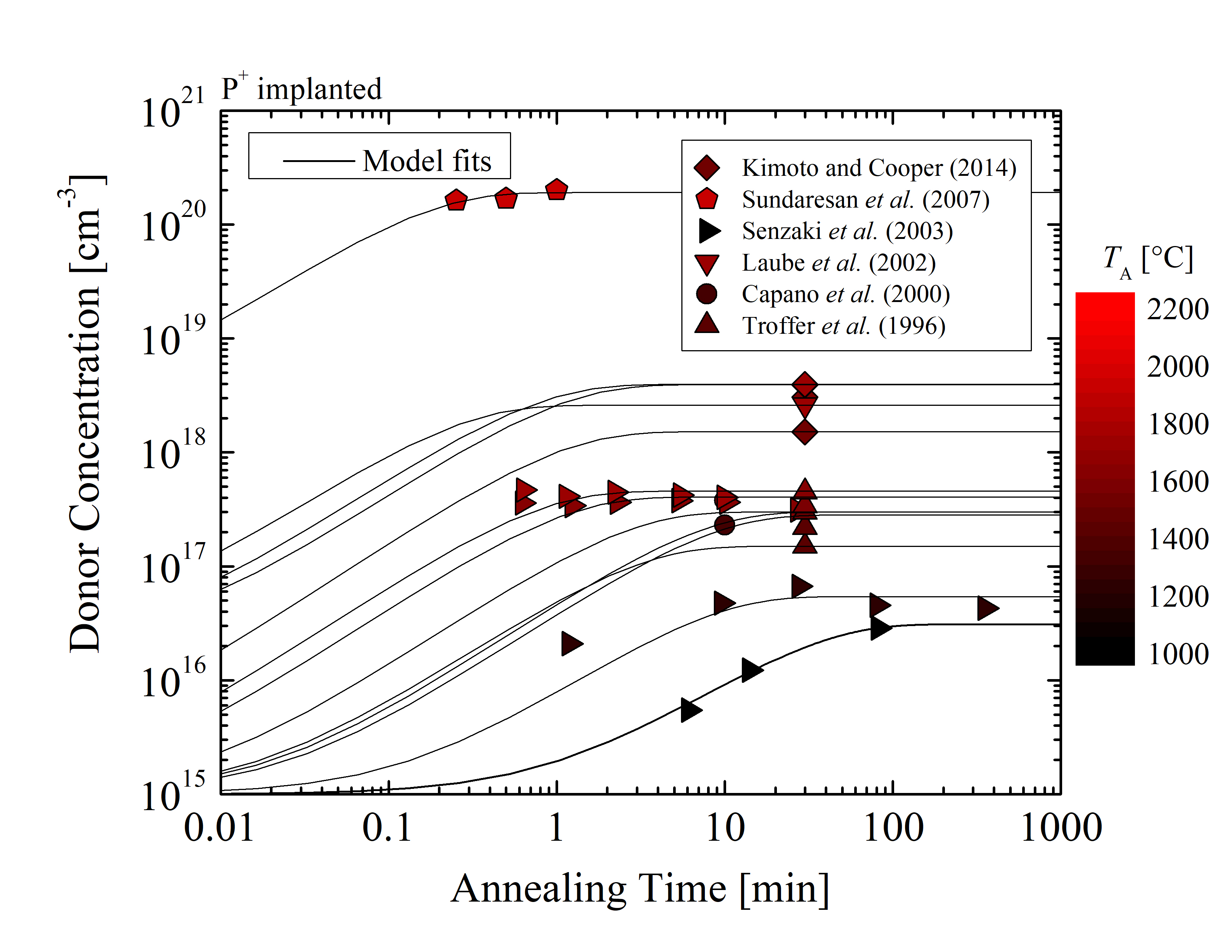
The preferred acceptor-type dopant species in SiC is Al for low resistivity applications [160], while the preferred donor-type dopant is P for high-dose implantations [161]. In addition, implantation and annealing steps of Al and P show potential for a wide utilization of SiC devices [161, 152, 137, 130], which is why the focus here is on Al- and P-implantation of 4H-SiC. A comprehensive collection of experimental data of various post-implantation steps of Al and P impurities in SiC has been gathered. The acceptor [162, 152, 134, 130, 163, 164] and donor [1, 164, 161, 138, 144, 141] concentrations have been obtained from experimental studies for various annealing temperatures, annealing times, and total implanted concentrations. The collected Al- and P-implanted data is plotted as a function of annealing time in Figure 3.17. As previously discussed, the experimental data has been selected such that identical crystal orientations, annealing ambients, implantation temperatures, and measuring methods are considered. This is particularly important as it enables proper model fitting for predicting the annealing temperature, annealing time, and total concentration [135]. It has been assumed that the different annealing methods (microwave, inductive, and restive heating) result in the same activation ratios [154]. All of the selected data is based on annealing in an Ar ambient. In addition, no differences in activation rates between 4H- and 6H-SiC are assumed [134]. According to the available experimental data, the error due to this assumption is less than 5% and is thus considered negligible.
Figure 3.17: (a) Acceptor and (b) donor concentrations as a function of annealing time for various total concentrations and annealing temperatures. The data has been taken from previous experimental studies for acceptor- [162, 163, 164, 152, 134, 130] and donor [1, 164, 161, 138, 144, 141]-type doping. The solid lines refer to model fits.
The transient model for electrical activation of dopants in SiC has been inherited and modified from the model for Si [53], which is described with a differential equation and represents the reaction of the dopants’ activation processes. The active concentration of dopants in SiC is [159] modeled by
\( \seteqsection {3} \) \( \seteqnumber {31} \)
\begin{equation} \frac {dC_\mathrm {act}}{dt} = -\kappa \left ( C_\mathrm {act} - \frac {C_\mathrm {tot}}{1 + \frac {C_\mathrm {tot}}{C_\mathrm {ss}}} \right ). \label {eq:transient_model} \end{equation}
Ctot is the total implanted concentration of dopants. Css and κ are solid solubility and characteristic reaction rate, respectively, and are the key parameters of the model, obtained by model fitting. In the case of SiC, Cact is approximated to be equal to the electrically measured (i.e., Hall and sheet resistance measurements) acceptor (NA) or donor concentration (ND), which originate from the ionized dopants only. Css is the limiting parameter for the total active concentration and κ is the limiting parameter for the reaction rate of the activation mechanism, i.e., the slope of the curve.
3.4.2 Calibration
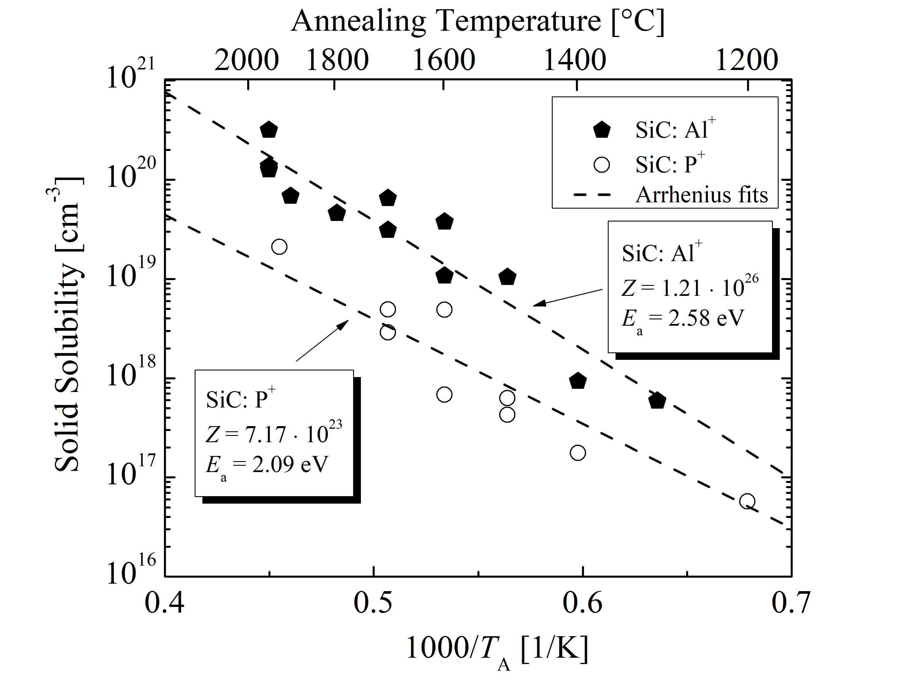
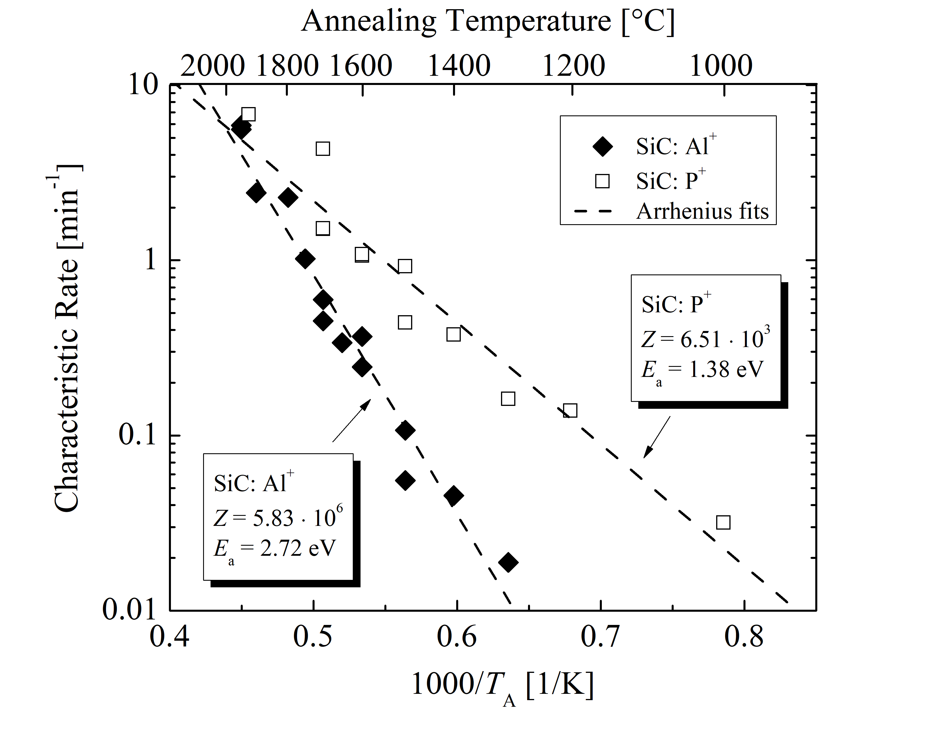
Several iterations of least squares approximation [165] have been performed for each individual data set to reduce the numerical error, when fitting the proposed activation model (3.31) to the data presented in Figure 3.17. The fitting parameters are Css and κ, which are individually obtained for each annealing temperature. The temperature-dependent parameters are then fitted with the Arrhenius equation [96] to ensure a continuous, interpolated, and extrapolated dependence on the annealing temperature. The calibrated Arrhenius parameters, i.e., activation energy Ea and pre-exponential factor Z, are summarized in Table 3.5.
The corresponding Arrhenius plots are shown in Figure 3.18. The activation energy for Al-implanted SiC is for both parameters (Css and κ) higher, compared to P-implanted SiC. Css is for relatively low temperatures (around 1150°C) identical for Al and P impurities. On the contrary, κ is for Al and P identical for relatively high temperatures around 1950°C. For the steady state solution of the model, i.e., solution for the thermal equilibrium, Css plays a significant role by defining the upper limits of the active concentration of the dopants for particular annealing temperatures. Moreover, Css varies up to an order of magnitude between the Al and P dopants for high temperatures. Additionally, the Arrhenius plots suggest that the solubility limit for Al-implanted SiC is higher, compared to P-implanted SiC.
Table 3.5: Arrhenius parameters, i.e., activation energy and pre-exponential factor, of the solid solubility and characteristic rate for Al- and P-implanted SiC.
| Css | κ | |||
| Dopant | Z [cm-3] | Ea [eV] | Z [min-1] | Ea [eV] |
| Al | 1.21 · 1026 | 2.58 | 5.83 · 106 | 2.72 |
| P | 7.17 · 1023 | 2.09 | 6.51 · 103 | 1.38 |
The proposed transient model, together with the obtained model parameters, enable the prediction of the transient active concentration or activation ratio after thermal annealing steps of SiC device fabrication. In the next sections the calibrated model is analyzed and the model results are validated based on the gathered experimental data. In particular, in-depth modeling and parameter aspects are discussed, followed by actual process simulations of representative PN-junction diodes including validations with experimental data. These analyses are concluded with evaluating the electrical characteristics via device simulations in comparison to experimental data.
3.4.3 Characterization
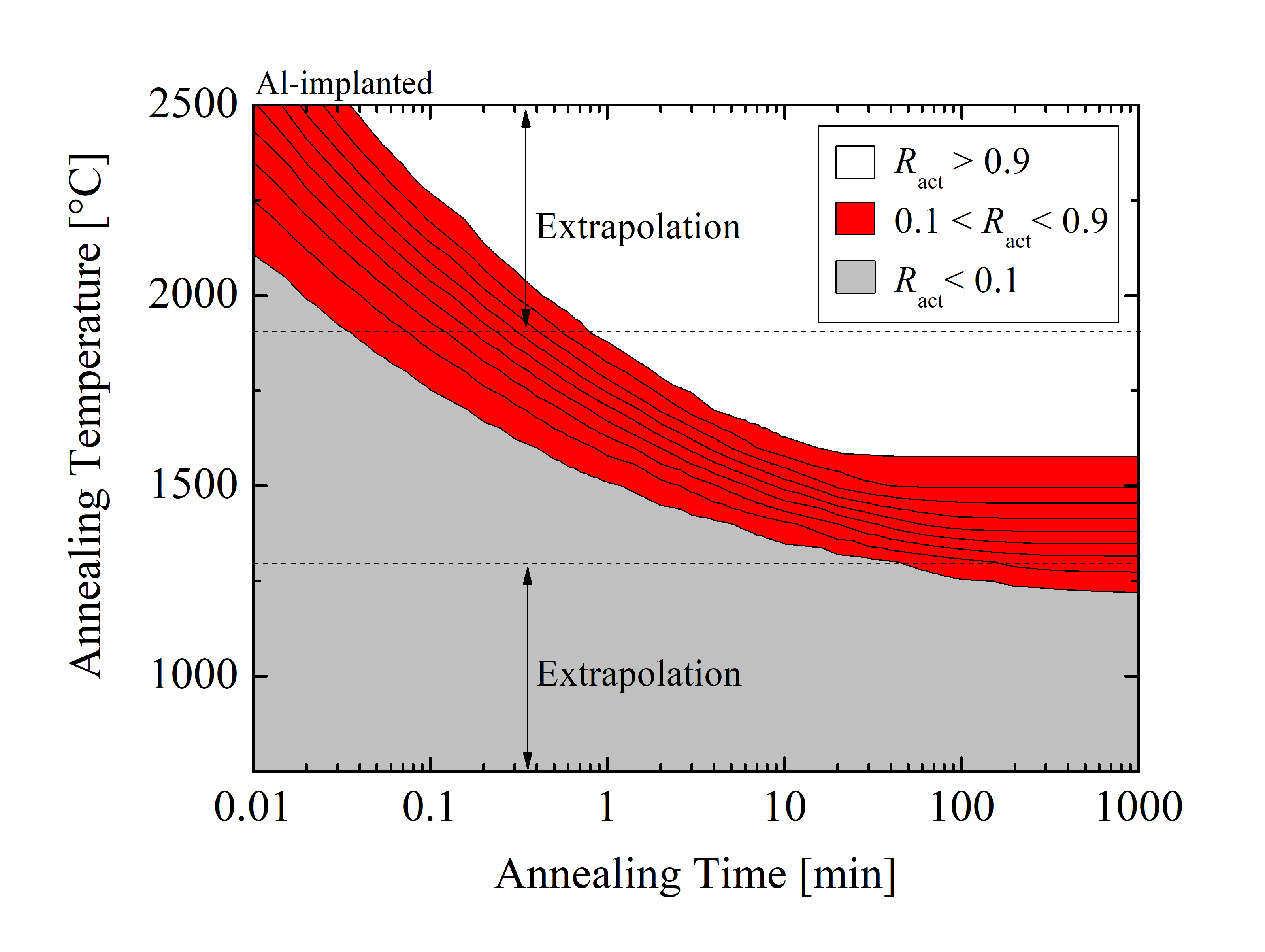
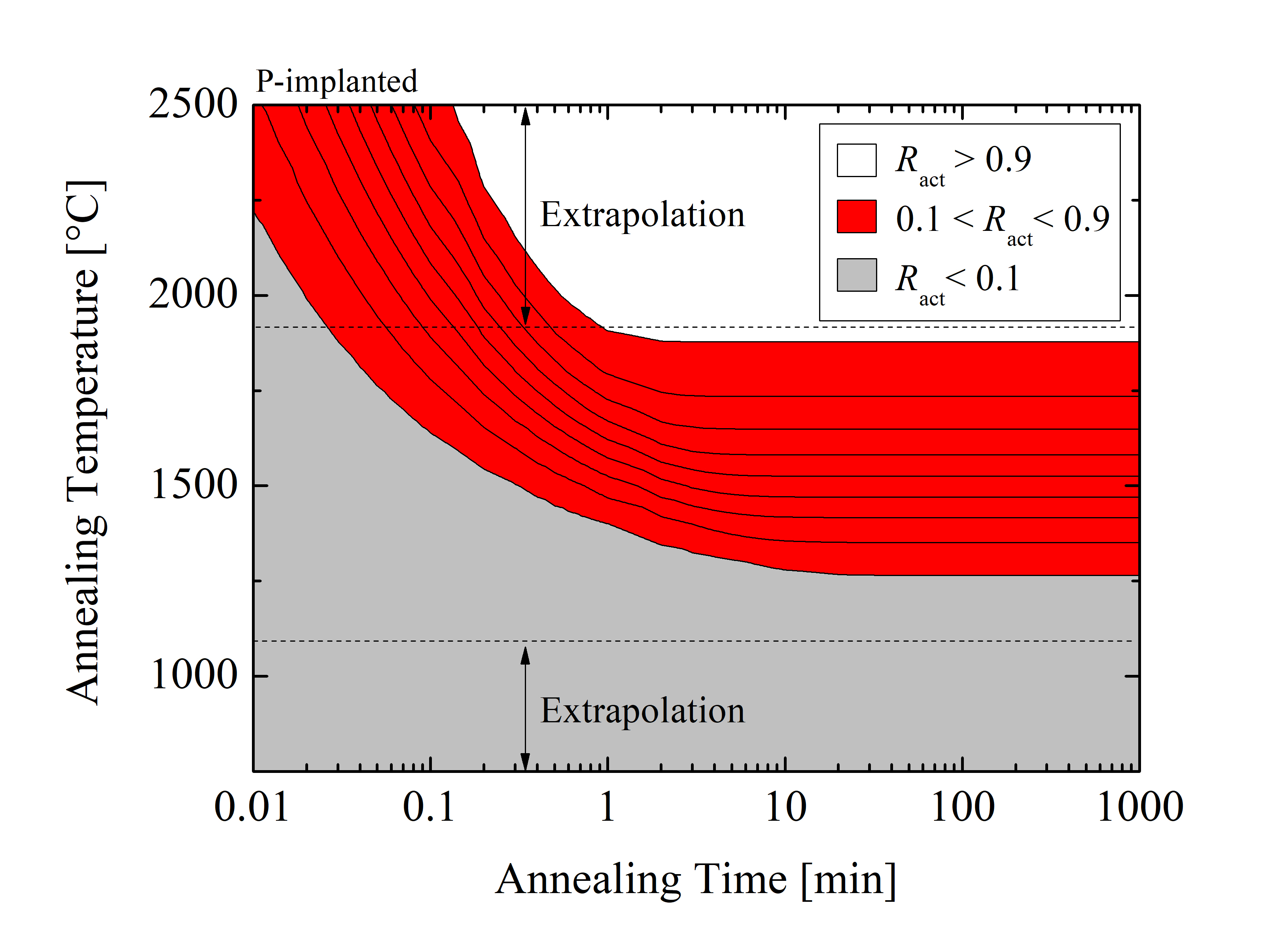
The transient activation model has been characterized based on two investigations, one considering constant implanted concentration with annealing time and temperature being the independent variables, and another considering a steady state with annealing temperature and total concentration being the independent variables. The steady state case refers to the dopant activation state where a prolonged annealing treatment will not affect the concentration of activated dopants. This is typically in the range above 1000 min of annealing time. The parameter studies have been performed based on numerous (i.e., 106) calculations of Al and P implantations in SiC, followed by various annealing steps. Phase diagrams of activation regions as a function of annealing temperature and annealing time are shown in Figure 3.19. Due to the Arrhenius fitting of the parameters, the results are extrapolated for certain annealing temperatures, shown with dashed lines.
The phase diagrams enable an estimation of the minimally required TA and tA to reach full (i.e., above 90%) activation. The phase diagrams additionally show that the phase region 0.1 < Ract < 1.0 is smaller for Al acceptors than for P donors. The difference in those areas indicates that P acceptors require less energy for activation than P donors, which is consistent with experimental findings [1]. Figure 3.19 in addition shows the steady states for different annealing temperatures. For instance, at 1700°C the steady state for Al acceptors is reached for an annealing time above ≈ 25 min and for P donors above ≈ 3 min, i.e., the activation ratio is not affected beyond these times.
In addition, it has been shown [159] that for high TA the initial activation speed is extremely high and decreases rapidly with time. This implies that the activation process for high TA is mostly significant for tA < 5 min. In contrast, for low TA the initial activation speed is a few orders of magnitude lower and decreases slowly, thus tA > 15 min is required for the effective activation of impurities. The activation process for TA = 1800, 2000, and 2200°C is almost instant and achieves > 90% activation. This indicates that rapid thermal annealing methods are indeed suitable for the activation of dopants in SiC, provided that the annealing temperatures are above ≈ 1700°C.
Figure 3.19: Phase diagrams of electrical activation as a function of annealing temperature and annealing time for (a) Al- and (b) P-implanted SiC. The simulations are performed for the total concentration Ctot = 1.0 · 1018 cm-3. The gray, red, and white regions refer to the low, intermediate, and high activation of SiC impurities, respectively. The dashed lines are the extrapolation boundaries.
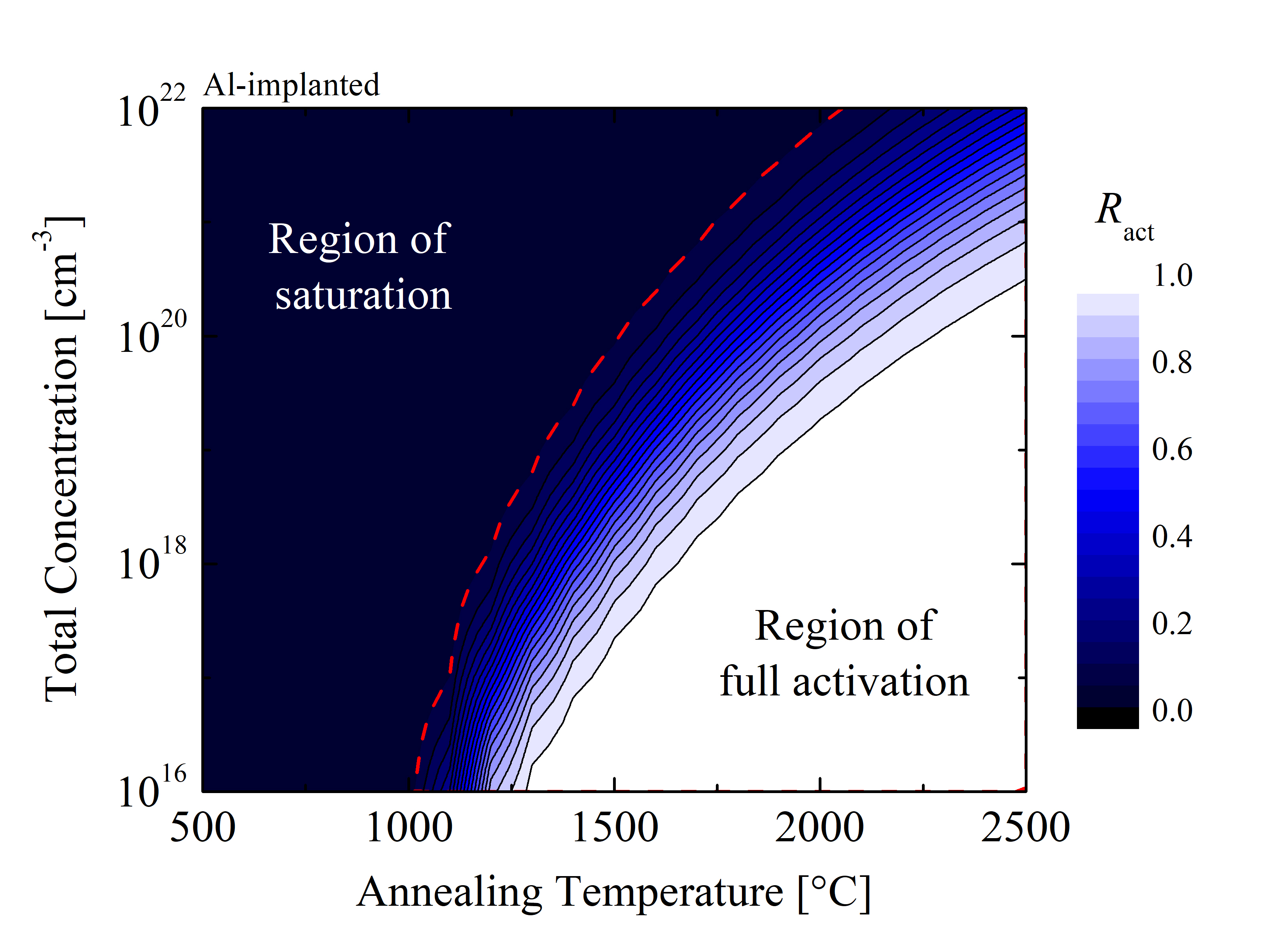
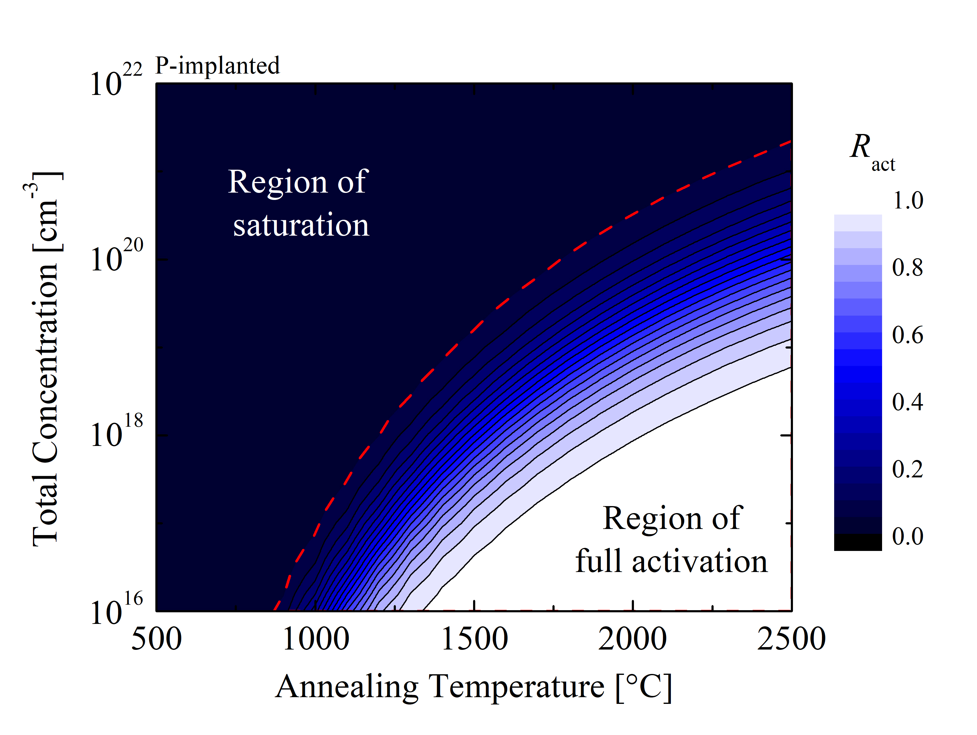
One of the significant issues of wide-bandgap semiconductors is that the rate of the dopant activation after high dose implantation (i.e., above 1018 cm-3) significantly decreases [152] and saturates [154]. In order to investigate the saturation effects due to high implantation doses, another parameter study is performed via calculating phase diagrams of activation regions as a function of annealing temperature and total implanted concentration, shown in Figure 3.20. These results suggest that the saturation region of the activation mechanism in SiC is temperature-dependent. As the annealing temperature increases, the boundary of the saturation region, shown with the dashed red lines, increases as well. This indicates that for annealing steps with high TA the doping doses can be a few orders of magnitude higher than with a low TA, while maintaining the same ratio of activation. The model predicts that annealing steps with TA below 1000°C for Al-implanted and 850°C for P-implanted SiC do not contribute to the improvement of electrical properties, regardless of the doping dose. The white region of the phase diagram, which refers to the full dopant activation, is larger for the Al-implanted SiC compared to P-implanted SiC. This indicates that a wider span of the parameter variety can be chosen for the acceptor-type doping, while maintaining the desired high activation ratio > 90%. These findings support the latest trend of Al being the preferable dopant for the SiC technology [166, 167, 160].
Figure 3.20: Phase diagrams of electrical activation as a function of annealing temperature and total concentration for (a) Al- and (b) P-implanted SiC. Simulations have been performed for an annealing time tA = 1000 min, i.e., steady state. The colors indicate various activation ratios (Ract) and the red dashed lines indicate the boundaries of the saturation regions.
3.4.4 Simulations
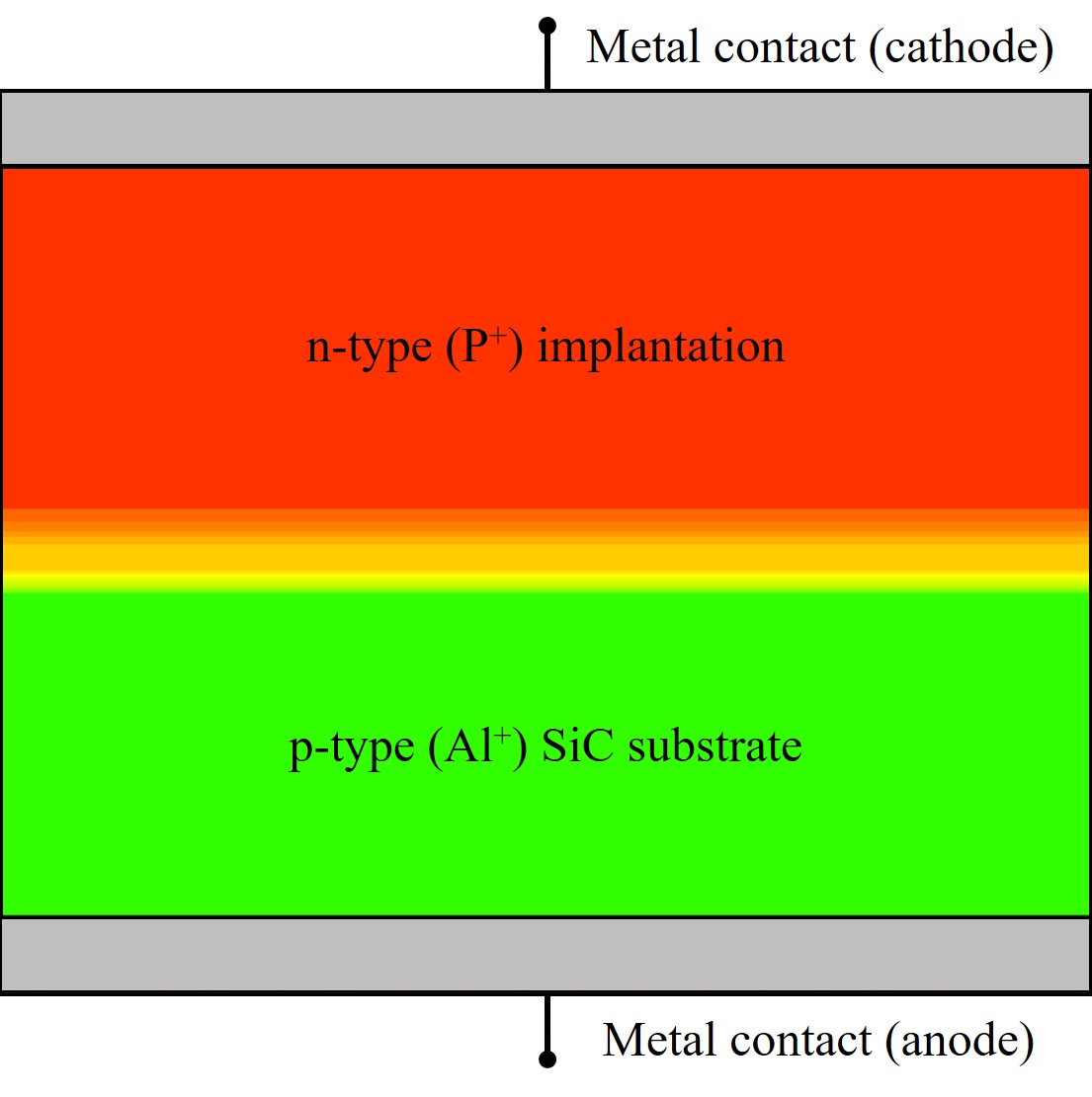
The transient model and the parameters from Table 3.5 have been implemented into Silvaco’s Victory Process simulator [53]. Various PN-junction diodes have been processed and evaluated according to model predictions. Each of the simulated PN-diodes varies with regard to the annealing temperature, annealing time, and/or total concentration. An exemplary device structure is shown in Figure 3.21 and the respective doping parameters are given in Table 3.6. The device processing setups are based on three different experimental investigations [161, 137, 141], which have been chosen to ensure a focused study of the annealing process. All of the setups include implantation of P in an Al-doped SiC substrate and a \((0001)\) Si-face crystal orientation. The simulated processing steps are: 1) p-type (Al-doped) SiC substrate. 2) n-type (P) implantation according to the chosen setup. The Monte Carlo implantation model from the Victory Process simulator has been utilized. 3) Deposition of SiO2. 4) Annealing of implanted species according to the experimental setups. This step includes the proposed model and parameters. 5) Removal of SiO2. 6) Deposition of metal for contacts on top and bottom of the device.
Table 3.6: Implantation setups for p-type SiC \((0001)\) Si-face.
| Setup | 1 | 2 | 3 |
| Reference | Schmid et al. [137] | Troffer et al. [141] | Senzaki et al. [161] |
| Substrate Al+ | 1.0 · 1016 | 1.3 · 1017 | 5.0 · 1015 |
| concentration [cm-3] | |||
| Implanted P+ | 70, 180, 320, | 70, 160, 280, | 40, 70, 160, |
| energies [keV] | 500, 750 | 450, 600, 800, | 180, 220, 250 |
| 1100, 1500, 2000 | |||
| Total fluence [cm-2] | 1.4 · 1016 | 1.3 · 1014 | 7.0 · 1015 |
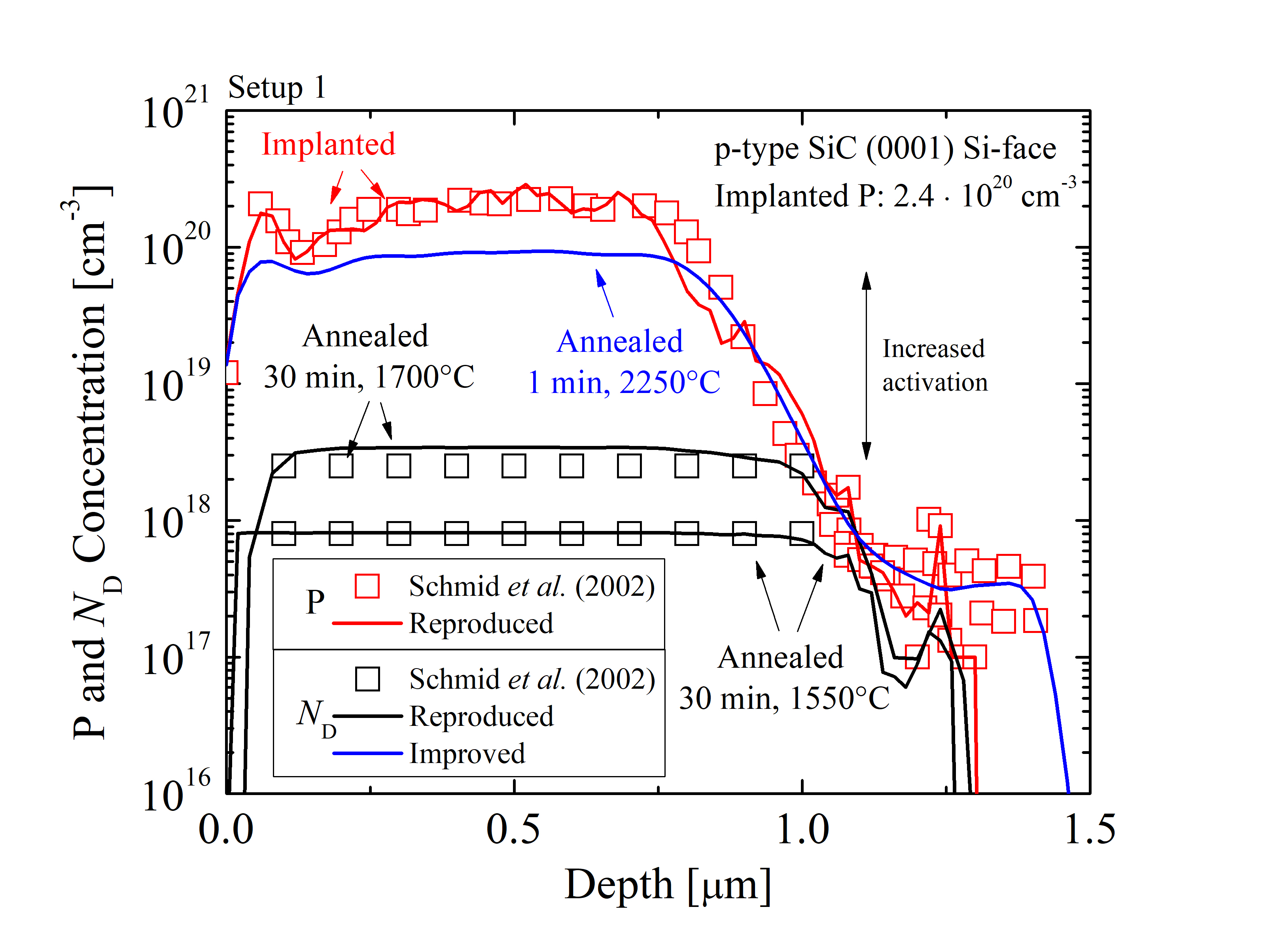
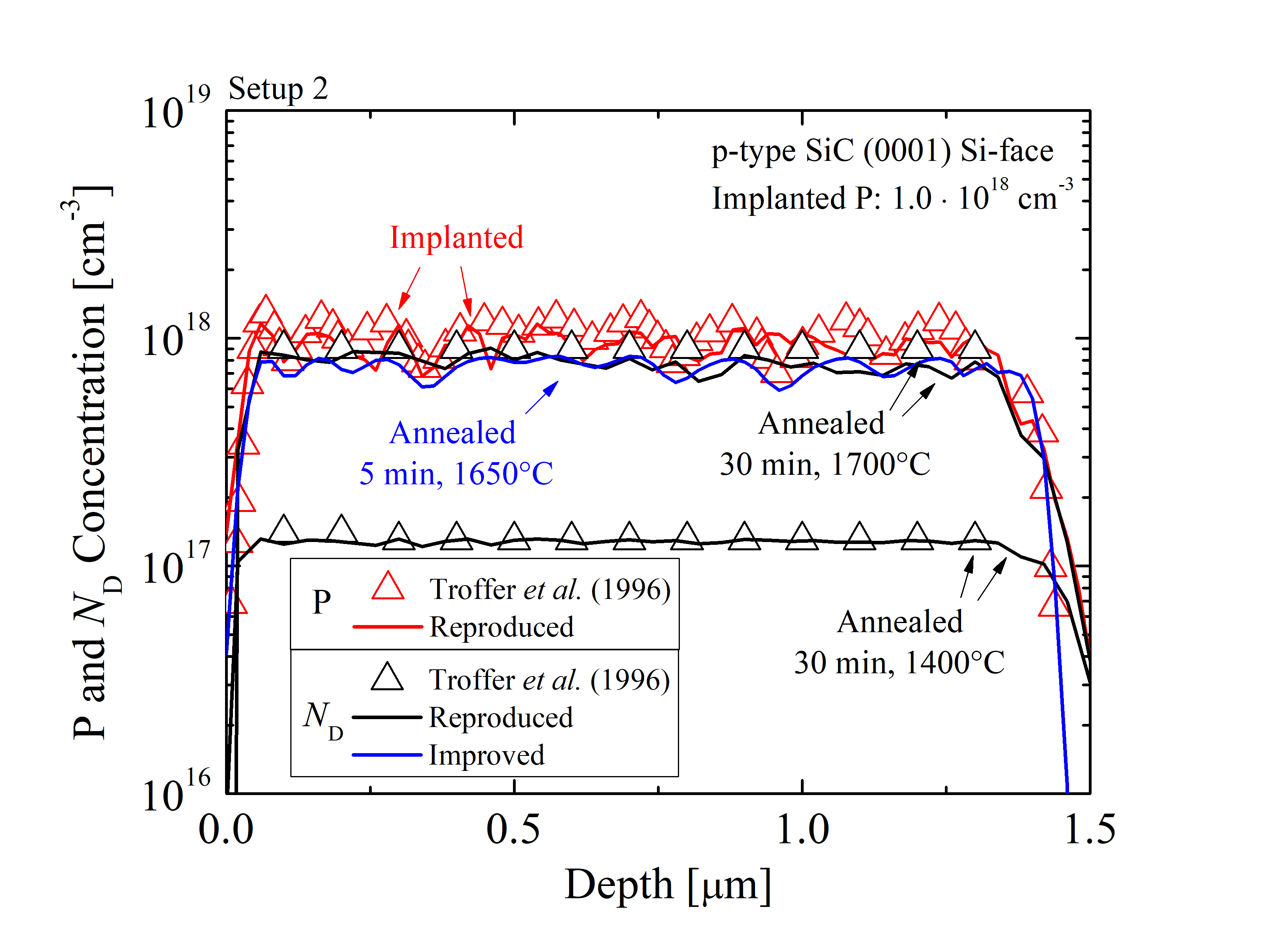
The depth profiles, i.e., P and donor concentration, of the two implantation setups and simulations are shown in Figure 3.22. The solid lines refer to the results from the process simulations and the symbols refer to the experimental findings. The red color indicates implanted profiles of both simulations and experiments. The simulated implanted profiles of Setup 1 (Figure 3.22 (a)) and Setup 2 (Figure 3.22 (b)) are identical to the profiles from the corresponding references. The implanted species are annealed for 30 min at 1700°C and 30 min at 1550°C in the case of Setup 1 and for 30 min at 1700°C and 30 min at 1400°C in the case of Setup 2. The deviation between the results from simulation and experiment for the annealed samples is in average σ < 3%. This indicates that the proposed model captures the key characteristics of the activation mechanism and provides an accurate prediction of the activation levels. It can be seen from Figure 3.22 (a) that a very low activation ratio of high-dose acceptor-type impurities is achieved after the typical annealing step, i.e., 30 min at 1700°C. Furthermore, an estimate of the required processing variables for sufficient (> 90%) activation is provided. Experimental methods have not been able to provide such an estimate due to technical limitations [137]. The prediction is based on the proposed model (blue lines) and suggests that the activation of high-dose implantation is significantly improved after an annealing step of 1 min at 2250°C. In the case of high-dose implantation ND has been increased from 3 · 1018 cm-3 to 6 · 1019 cm-3. Moreover, such simulations can provide an estimate for the shortest annealing time and lowest annealing temperature, which result in a desired active concentration. For instance, for Setup 2, it is evident that an annealing step of 5 min at 1650°C is sufficient to achieve an identical activation as compared to annealing for 30 min at 1700°C. This underlines that already small temperature variations (e.g., 50°C) have a strong impact on the activation process.
According to the obtained depth profiles of Setup 1 and Setup 2, device simulations have been performed to characterize the electrical properties of the implanted SiC after the investigated annealing steps. In order to characterize the processed PN-diodes, the carrier concentration as a function of sample temperature is investigated and shown in Figure 3.23. The comparison of the experimental data (red symbols) and simulation results (black lines) clearly demonstrates a very low deviation, in average σ < 1%. The PN-junction diode, processed with the previously proposed annealing step from Setup 1, shows improved device characteristics (Figure 3.23 (a), blue line). The carrier concentration is significantly increased by one order of magnitude, which provides better overall device operation. Moreover, the diode, which is fabricated with the proposed annealing step from Setup 2 (i.e., reduced time and temperature), shows an almost identical behavior (Figure 3.23 (b), blue line) as the diode with the non-modified annealing step. Small variations between the two annealing steps are evident in extreme operation temperatures, i.e, below 150 K and above 700 K, but are almost identical in the typical device operation regime, i.e., 200 - 600 K. Thus, the shorter annealing step is sufficient to achieve the same characteristics yet within considerable shorter time.
Figure 3.23: Carrier concentration as a function of sample temperature utilizing implantation (a) Setup 1 and (b) Setup 2. The symbols refer to experimental data from [137, 141], the black lines are simulation results from reproduced depth profiles, and the blue lines are simulation results from predicted depth profiles. The reproduced and predicted depth profiles are shown in Figure 3.22.
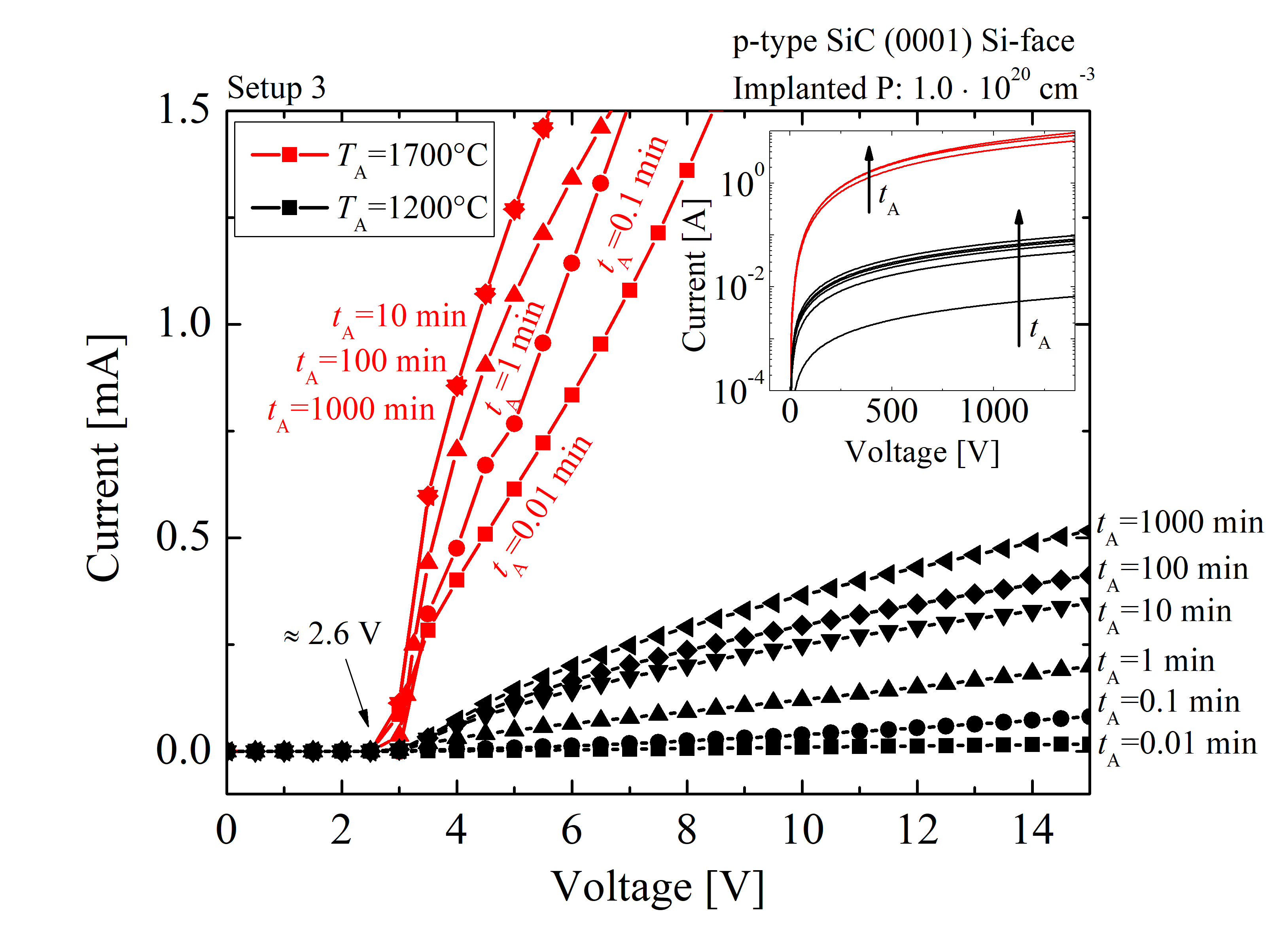
The simulation capabilities of the transient model are further evaluated by processing SiC diodes based on the implantation and annealing parameters of Setup 3 (cf. Table 3.6). Numerous process simulations of the PN-junction diodes have been performed followed by device simulations to obtain the current-voltage (IV) characteristics of each individual device. This approach, i.e., numerous process simulations, which are distinctive in the annealing variables only, provides a focused investigation of the annealing steps. Various tA from 0.01 min to 1000 min at TA from 1200°C to 1700°C have been investigated. The IV plots for various tA and TA are shown in Figure 3.24. For the sake of readability, only the two extreme conditions are shown, i.e., TA = 1200 and 1700°C. The knee voltage is, regardless of the processing conditions, ≈ 2.5 V, which is approximately three times higher than that of an equivalent diode based on Si. It becomes clear from the results, that both annealing variables, TA and tA, significantly affect the slope of the IV characteristics and consequently the resistance of the samples. The IV plots (Figure 3.24) have been used to calculate the resistance-time characteristics of each individual device. The sheet resistance is obtained from the slope of the IV plots and the diode geometries for various tA and TA, as shown in Figure 3.25. For TA > 1600°C the sheet resistance decreases until tA ≈ 1 min. This implies that for high annealing temperatures a rapid annealing step is sufficient. In this case no significant decrease of the sheet resistance is observed for tA > 1 min. On the other hand, low-temperature annealing shows a continuous decrease of the sheet resistance over 1000 min. The figure in addition suggests that the sheet resistance is reduced for more than 500 Ω/sq between the annealing step of TA = 1200°C and 1700°C. The comparison of the results (solid lines) to the experimental findings (symbols) shows a very good agreement, i.e., in average less than 5% deviation. This implies that the proposed model provides a very accurate prediction of the annealing temperature-dependent sheet resistance of SiC devices.

