2 Thermal Oxidation
This chapter discusses key contributions made to modeling and understanding of SiC oxidation mechanisms, in particular, oxidation growth rates, orientation-dependent interpolation method, and first principle simulations. But first, fundamentals of the thermal oxidation process are introduced in the following.
One of the essential steps in fabrication of electronic devices is thermal oxidation [1], which is a chemical process to produce ten to hundred nanometer thick oxide layers, usually SiO2, on the surface of a wafer. The produced SiO2 layers find their application in insulating and protecting layers as well as gate oxides of MOSFETs. The oxidation technique forces an oxidizing agent to diffuse into the wafer at high temperatures (usually above 700°C) in an oxidizing environment, such as O2, steam, or nitric oxide (NO) [44]. A native oxide layer of a thickness of up to 2 nm rapidly forms on the surface. After this initial native oxide layer, the oxidation rate is significantly reduced and the oxidation effectively stops after a final thickness in the order of a few hundreds of nanometer is reached. The oxidation stops when oxygen molecules at particular oxidation temperatures do not have enough energy to diffuse through the formed oxide layer, which acts as a passivation layer for the oxidation process [49].
Thermal oxidation is accomplished using an oxidation furnace which provides the heat needed to elevate the oxidizing ambient temperature. A furnace typically consists of 1) a cabinet, 2) a heating system, 3) a temperature measurement together with a control system, 4) fused quartz process tubes, where the wafers undergo oxidation, 5) a system for moving process gases in and out of the process tubes, and 6) a loading station used for loading (or unloading) wafers into (or from) the process tubes. The heating system usually consists of several heating coils which control the temperature around the furnace tubes. The wafers are placed in quartz glassware known as boats which are supported by fused silica paddles inside the process tube. A boat can contain many wafers, typically 50 or more. The oxidizing agent (O2 or steam) then enters the process tube through its source end, subsequently diffusing to the wafers where the oxidation occurs. Typically, an additional gas species (e.g., NO) is added to the oxidizing ambient in order to increase the quality of the grown oxide, i.e., to reduce the density of interface traps [1, 55]. A schematic representation of a thermal oxidation furnace is shown in Figure 2.1.

SiO2 layers can be also produced with various deposition techniques, e.g., CVD which is typically less expensive compared to thermal oxidation. However, for the deposition process it is extremely challenging to be able to accurately control deposition for oxide thicknesses below 10 nm. Another disadvantage is the poor electrical property of the interface between a deposited oxide layer and the underlying material (e.g., Si or SiC). In addition, the density of the deposited oxide is lower compared to one of the thermally grown oxide [44]. The details of the thermal oxidation mechanism and the properties of SiO2 are discussed in detail in the following sections.
2.1 Silicon Dioxide
SiO2 offers many desired properties and advantages for semiconductor electronic devices, particularly MOSFETs. SiO2 layers can be grown thermally on many desired semiconductor materials (such as Si and SiC) and are resistant to most of the chemicals used in device fabrication processes [44]. Oxide layers can be in addition relatively easily patterned and selectively dry or wet etched. Commonly, oxides are used to prevent in- or out-diffusion of dopants or other impurities from the wafer [49]. SiO2 has an indispensable thermal stability for process and device integration (up to 1600°C). Furthermore, SiO2 is an excellent insulator with a wide-bandgap of ≈ 8.9 eV and a high dielectric strength of ≈ 107 V/cm [56]. The key properties of SiO2 are shown in Table 2.1. The bandgap of SiO2 is more than seven times larger compared to Si, which makes it very suitable for, e.g., dielectric isolation.
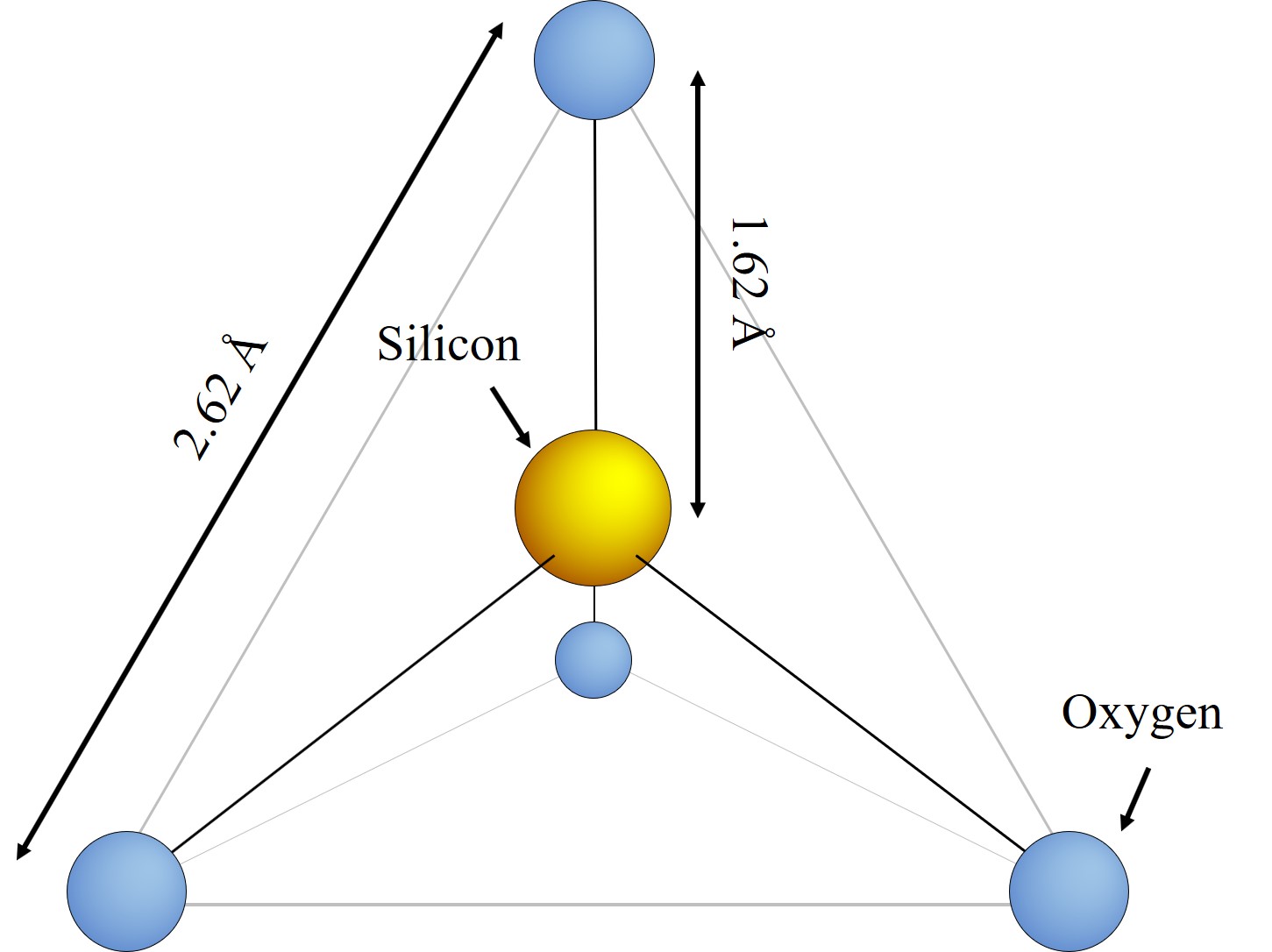
The structure of SiO2 is constructed of four oxygen atoms and a single Si atom in the centre of a tetrahedron. The length of a Si-O bond is normally 1.62 Å and the distance between the oxygen atoms is 2.62 Å. The distance between the two Si atoms, i.e., between the two unit cells, in a complete oxide structure is typically 3.1 Å. The molecular structure of a single SiO2 molecule is shown in Figure 2.2.
Table 2.1: Relevant chemical and electrical properties of SiO2 including molar mass, melting point, thermal density, thermal conductivity, relative dielectric constant, and energy bandgap [56].
|
Molar Mass |
60.08 g/mol |
|
Melting Point |
1713°C |
|
Thermal Density |
2.18-2.27 g/cm-3 |
|
Thermal Conductivity |
3.2 · 10-3 W/(cm K) |
|
Relative Dielectric Constant |
3.7-3.9 |
|
Dielectric Strength |
107 V/cm |
|
Energy Bandgap |
8.9 eV |