|
It is essential for
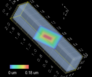
three-dimensional simulation of semiconductor technology process steps
to be able to deal with non-planar surfaces which describe the complex
geometry of modern devices. One of the methods for dealing with
surfaces is the level set method. This
method describes the propagation of material surfaces in the production
processes of semiconductor technology processes such as etching and
deposition. For this
method we use a rectangle grid, and the needed surface information is
calculated at each point of this grid. Examples for this surface
information
are the relative distance of the grid points to the surface and the relative
speed of the surface.
A quick algorithm for calculating the distance of every grid point to
the material surface is implemented. The complexity of this algorithm
is O(rN + M), where N is grid points, M is the number of edges and vertices
and r is calculation-effectivity dependent. This implementation and
other future implementations are based on the Wafer-State-Server. This
ensures compatibility with other tools developed at the institute.
Future work will also include surface grid generation. The quality of
the volume grid generation depends on the generation of the surface
grid, which must accurately represent the device geometry.
This shows that surface grid generation has a crucial meaning for the
whole simulation of the etching or deposition process.
|