|
Due to the increasing
complexity of interconnects and devices in microelectronic structures,
optimization problems in TCAD applications are steadily becoming more
complex.
Thus, simulations and, therefore, optimizations become increasingly
more time-consuming, especially if three-dimensional structures are
considered. Since current workstations offer increased performance at
steadily decreasing costs, they can be easily included as computational
nodes in existing simulation and optimization clusters. This allows
genetic optimization algorithms which are normally very time-consuming
to be employed.
However, these new approaches require tools that are able to manage the
available network resources efficiently and avoid inconsistencies and
overloads of certain simulation nodes. Therefore, the integrated
simulation and optimization framework SIESTA
(Simulation Environment for Semiconductor Technology Analysis) has been
developed at the Institute for Microelectronics. It integrates a global
network resource management and a variety of optimizers and simulators
to combine the advantages of optimization strategies like those of
gradient-based and genetic optimizers. The software concept of SIESTA
has been completely redesigned in order to improve and extend the
interfaces to graphical user interfaces (GUIs), optimizers, and
simulators. Thus, a loosely-coupled system was created with only minor
restrictions for external software tools. Additionally, fault tolerance
has been included in the interface structures to provide a stable
operation.
With this variety of tools, the capabilities of the simulation
framework SIESTA include investigations and
optimizations of parameters for semiconductor process and device
simulation. Furthermore, this framework allows inverse modeling of
devices and technology processes, which is useful for the extraction of
specific material and process parameters. The required information
includes measured data and an appropriate base model which allows SIESTA
to optimize the chosen parameters automatically. This technique has
already produced excellent results in process and device optimizations.
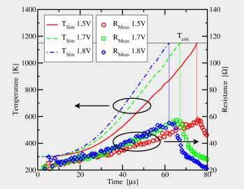
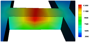
Currently, thermal effects in polycrystalline semiconductors and
multi-level interconnect structures are being investigated. The
three-dimensional interconnect simulator STAP is used
to predict critical temperatures in some parts of the semiconductor. At
high temperatures, however, conventional models do not predict the
change of the electrical behavior correctly. Therefore it is necessary
to include advanced models in device simulators which are valid in
these temperature ranges. SIESTA can be used to
calibrate analytical models included in device and circuit simulators.
Additionally, new graphical user interfaces are developed to improve
the usability of SIESTA. These tools enable the user
to setup, control, and interact with SIESTA.
|