|
Usage of strained
silicon can improve performance of both NMOS and PMOS devices.
This design option is already employed in the present 90nm technology
node. Physical models and parameter values of TCAD tools have to
be carefully upgraded to cover the properties of the strained Si/SiGe
material
system. A main goal of this project is the development of mobility
models for strained silicon. A physically-based bulk mobility model has
been developed, which takes into account the strain-induced valley
splitting and the resulting valley repopulation. The model is based on
ideas developed by Manku and Nathan. A term accounting for inter-valley
scattering has been added. This effect has been found important to
improve agreement with experimental data and bulk Monte Carlo (MC) data
produced using VMC.
Quantitative analysis of hole transport in strained semiconductors
requires a numerical representation of the band structure. For this
purpose, a full-band MC kernel is currently being developed. Momentum
space is discretized using tetrahedrons, which allow
effective interpolation and integration of the equations of motion.
The band structure is calculated by a solver implementing the nonlocal,
empirical pseudopotential method.
Development of an MC simulator for the transport in channels has
continued.
The simulator reads in the sub-band energies and overlap integrals
computed by a self-consistent Schroedinger-Poisson solver. Using
adjusted surface roughness and phonon scattering parameters
the simulator reproduces the universal electron mobility curve
for unstrained silicon and gives reliable predictions for
strained silicon channels. The Lombardi model is used as a starting
point for the development of an analytical, strain-dependent surface
mobility model.
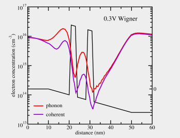
A new project on the modeling of silicon FETs near the scaling limit
has been commenced. The recently developed MC module for the
Wigner-Boltzmann equation will be applied. Goals are the inclusion
of size quantization effects and a more realistic band structure
in the transport model. Recently, the multi-valley band structure
of silicon has been implemented in the Wigner MC module, which has
originally been benchmarked on GaAs-based resonant tunneling diodes.
Various architectures of carbon nanotube (CNT) FETs have been
studied using Minimos-NT. Assuming ballistic transport, a
Schroedinger-Poisson solver is used to analyze the Schottky barriers.
The current is then calculated using the Landauer-Buettiker formula.
The charge on the tube can now be taken into account self-consistently.
To optimize the off-state characteristics of the CNT-FET, a dual-gate
structure has been proposed. The second gate effectively suppresses
hole tunneling at the drain contact.
|