To understand the influence of the edge
topography on the device characteristics, which is important for highly
integrated ICs, an accurate three-dimensional topography simulator is
required. However, topography simulation is still facing many
challenges which limit its general applicability and usefulness.
Furthermore, three-dimensional topography simulation tends to be very
CPU and memory intensive.
Various surface representation algorithms have been used for the
development of three-dimensional topography simulations. The most
efficient algorithm is the level set algorithm. In this algorithm the
location of an interface is the zero level set of a higher dimensional
function which is called level set function.
Based on an efficient and precise level set method including narrow
banding and extending the speed function in a sophisticated algorithm,
we have developed a general three-dimensional topography simulator for
the simulation of deposition and etching processes. The simulator is
called ELSA (Enhanced Level Set Applications) and
works efficiently concerning computational time and memory consumption,
and it simultaneously ensures high resolution. The speed of the
simulator compared to conventional level set based topography
simulators has been improved in several steps, e.g., in initialization,
visibility determination, and solving the radiosity matrix.
In addition, the calibration of our two-dimensional topography
simulator using measurements of a TEOS CVD process has been and is
still being done using various transport models. The parameter
calibration and optimization are carried out with SIESTA
(Simulation Environment for Semiconductor Technologies Analysis).
|
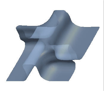
Three-dimensional deposition simulation of
a
T-Junction as initial boundary
|