|
MOS device technology is undergoing a constant shrinking process.
According to the International Technology Roadmap for Semiconductor
Devices 2003, the printed gate length will scale down to 28 nm by 2009.
Fully-depleted devices such as FinFETs emerged as promising candidates
to replace bulk MOS field-effect transistors due to their immunity
against short-channel effects. FinFET devices with a gate width of only
6.5 nm have already been reported. In contrast to bulk MOSFETs, these
devices inherently require three-dimensional investigations.
Unfortunately, with shrinking device dimensions classical device
simulation becomes more and more inaccurate. A rigorous
Schrödinger-Poisson solver would be necessary to accurately
describe the device behavior. As such simulations are computationally
extremely demanding, due to the large number of grid points in
three-dimensional problems, they are normally not appropriate. Instead,
classical device simulations with additional quantum correction models
can be used.
The drift-diffusion model estimates an exponential increase of the
carrier concentration towards the Si/SiO2 interface. Quantum mechanical
simulations show, however, that the charge centroid is located several
angstroms away from the interface. Therefore, several quantum
confinement models have been proposed.
The density-of-states (DOS) correction reduces the DOS at the Si/SiO2
interface, which is classically modeled as a constant value throughout
homogenous materials. Therefore, the carrier concentration at the
interface is reduced. An alternative approach is based on the first
eigenvalue of the triangular energy well at the interface. The band
edge of the conduction band at the interface is set to this eigenvalue
and therefore increases the bandgap.
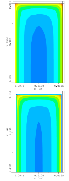
The figure shows the carrier concentration within the fin of a FinFET
structure. The simulations have been performed with classical
drift-diffusion simulation and the band edge correction model,
respectively.
|