|
In recent years, the
performance improvement of VLSI circuits has been attributed to the
continuous shrinking of feature size or alternatively to the
introduction of new device structures or materials. In this regard,
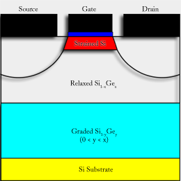
strained Si, due to its different material properties and excellent
compatibility with conventional Si technology, has emerged as a
promising material. The introduction of strain into the Si layer leads
to a splitting of the valence and conduction bands, resulting in
enhancement of both the electron and hole mobility. Enhancement ratios
as high as 70% and 100% as compared to unstrained Si have been both
theoretically verified and experimentally measured for electrons and
holes, respectively.
In order to study the performance of strained devices, a reliable set
of models for parameters such as mobility, energy bandgap and
relaxation times is required for strained Si. The Monte Carlo method
serves as an important tool for studying the effect of strain on device
characteristics. Based on the Monte Carlo simulations, the required
models for the strained Si/SiGe material system can be obtained. These
models are to be implemented in Minimos-NT and then
used to investigate and design different strained Si device structures.
The bulk mobility enhancement ratio for electrons has been fit to the
experimental data by adjusting the inter- and intra-valley coupling
constants. An analytical expression for the bulk mobility has been
suggested which fits the MC data. This analytical expression for the
bulk mobility along with another model for the material composition
dependence of the mobility for relaxed SiGe has been implemented in Minimos-NT.
Also, it has been possible to fit the experimental data for effective
electron mobility versus effective field for strained Si, which shows a
large variation, using the well known Lombardi mobility model. Future
work will concentrate on modeling of the various parameters based on
Monte Carlo results, with special focus on the surface mobility and
obtaining device characteristics.
|