|
Strain in silicon is
able to enhance the effective mobility of both n-channel and p-channel
MOSFETs by around 70% and 100%, respectively. In SOI and DG MOSFETs the
thickness of the Si substrate has a major impact on the device
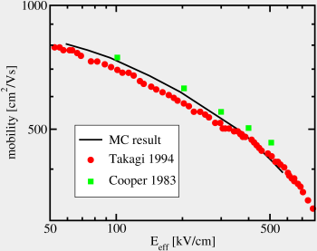
performance. Accurate models for the mobility of DG-, SOI-, or strained
Si/SiGe MOSFETs require a simulation of the inversion layer mobility.
The strong confinement leads to the quantization of the electron (hole)
state normal to the interface and the conduction (valence) bands split
into a system of discrete subbands. In the direction parallel to the
interface the charge carriers behave like free particles. This system
is called 2D electron gas and exhibits different scattering rates than
the bulk
case and additional scattering mechanisms caused by surface roughness
and oxide charges. The scattering mechanisms have been introduced in an
MC simulator suited for the simulation of the inversion layer mobility.
In order to extract the universal mobility curves, the MC simulator has
been coupled to a Schrödinger-Poisson solver.
The full-band structure is an indispensable ingredient of hot-electron
and hole transport in general. The MC simulator VMC, which is based on
the approximation of non-parabolic bands, is being extended to allow
full-band MC simulations. A band structure simulation tool based on the
non-local empirical pseudopotential method with relativistic
corrections
was extended to extract the band structure of strained silicon layers
grown on silicon-germanium substrates. This will allow the simulation
of novel devices including strain effects in two and three dimensions.
The performance of Schottky barrier carbon nanotube field effect
transistors (CNTFETs) depends critically on the device geometry.
Asymmetric gate contacts, the drain- and source contact thickness, and
non-homogeneous dielectrics above and below the nanotube influence the
device operation. CNTFETs were optimized with respect to the
subthreshold slope, high on-off ratio, and large on-currents. It was
shown that the use of a thin needle-like source contact is favorable,
whereas large drain contacts can decrease the off-current. The best
performance improvements can be achieved using asymmetric gates
centered above the source contact, where the position and length of the
gate contact varies with the oxide thickness and high-k materials on
top of the CNT and low-k materials below the tube. It was demonstrated
that by optimization of the geometry the subthreshold slope can be
reduced by
a factor of two, reaching a value of 100 mV/dec for devices with oxide
thicknesses of 5 nm.
|