


2D Materials and Devices
Following the conventional scaling paradigm, according to the IRTS roadmap, standard 3D silicon technology will have to consist of only a small number of atoms. In fact, the thickness of dielectric layers in MOS transistors already reached thicknesses of only a few layers a decade ago, which necessitated the introduction of high-k dielectrics. However, continuation of these scaling efforts is extremely challenging as ultra-scaled channels will have low mobilities. In addition, variability and the quality of the amorphous interfacial layers will be more and more difficult to control.
As a possible way out, the use of 2D materials has been suggested. These 2D materials ideally consist of planar crystalline layers which can be stacked in a more or less arbitrary manner to create novel device structures. Following in the wake of graphene, hundreds of 2D materials have been discovered and their properties and potential urgently awaits exploration.
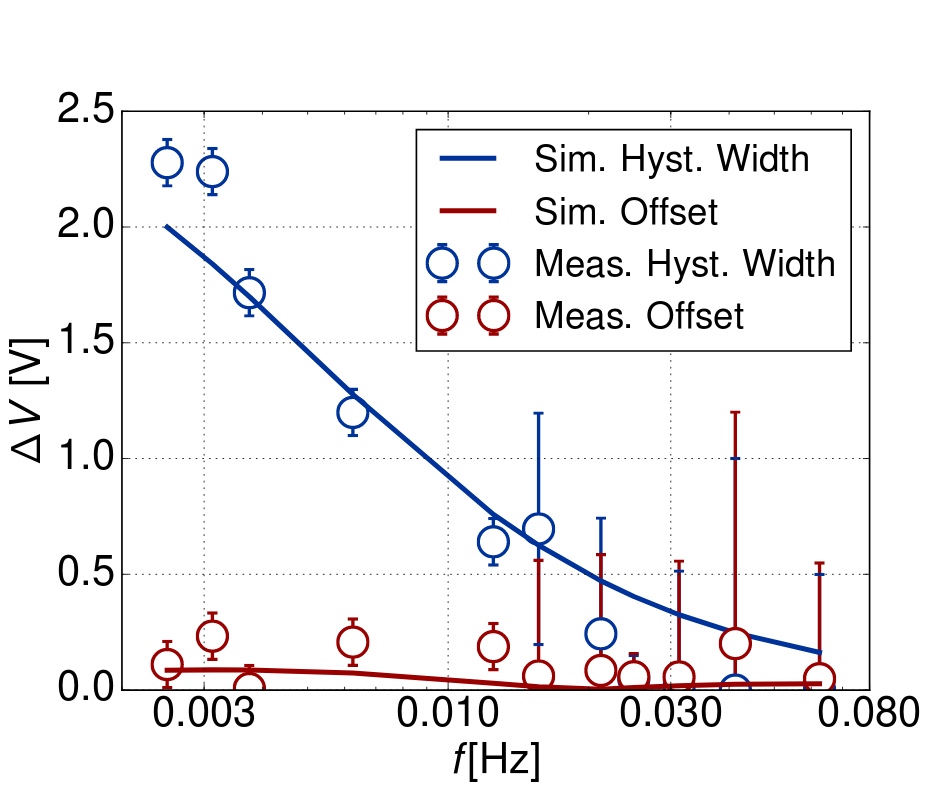
Since fabrication of these 2D devices faces numerous challenges, their theoretical exploration is considered a must. We have transferred and augmented our know-how as we have moved from 3D to 2D material systems and extended our tools accordingly. A particular focus of our work is on the non-idealities, such as defects, which lead to reduced mobility, hysteretic behavior (see Fig. 1), and long-term reliability issues.