2D Materials and Devices
The scaling paradigm of the IRDS roadmap dictates that standard 3D silicon technology must be scaled down to channels measuring only a dozen atoms in thickness. In fact, the thickness of dielectric layers in MOS transistors has already reached values of only a few atomic layers a decade ago. This development necessitated the introduction of high-k dielectrics. Nevertheless, the continued downscaling of also the channel material is extremely challenging as the mobilities in thin silicon channels are degraded. Furthermore, controlling the variability and the quality of amorphous interfacial layers is projected to become increasingly more difficult.
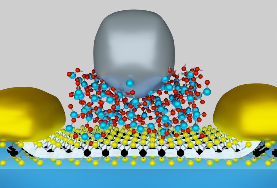
As a possible solution, the use of two-dimensional (2D) materials has been suggested, for example as a channel material in scaled transistors, see Fig. 1. These two-dimensional (2D) materials consist of layered crystals that can be stacked in numerous ways to create novel device structures. After the discovery of graphene, a plethora of two-dimensional (2D) materials have been identified, and their properties and potential await exploration.
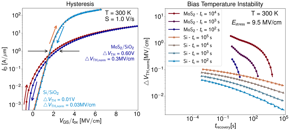
Given the numerous challenges associated with the fabrication of these 2D devices, their theoretical exploration is considered a must. We have transferred and augmented our know-how as we have moved from 3D to 2D material systems and extended our modeling tools accordingly. A key challenge in the field of 2D channel-based transistors is the identification of an optimal gate insulator. A high-quality gate insulator is essential for ensuring optimal capacitive gate control and for minimizing gate leakage currents. Furthermore, in order to mitigate variability, it is essential to create a high-quality interface and to control the threshold voltage well. 2D devices operate reliably if the observed hysteresis and the long-term drifts induced by border traps are small, see Fig. 2. Moreover, the dielectric should withstand elevated electric fields over an extended duration.Two promising groups of insulators for 2D transistors that have been the focus of our studies are native oxides to 2D materials and fluorides. Another focus of our research is on non-idealities, such as point defects in the gate insulator. These defects can lead to reduced mobility, hysteretic behavior, random telegraph noise, large variability, and long-term reliability issues like the bias temperature instability.