


Semiconductor Sensors
While aggressive transistor scaling has been at the forefront of developments in the semiconductor industry for decades, there is currently an increasing demand for added functionalities on a single device, usually referred to as More-than-Moore integration. This is most evident in the rapid development of integrated smart sensors in many industries, including smart homes, auto, and health, and the rise of wireless sensor networks and the Internet of Things. Our research encompasses a broad variety of materials and devices for various environmental and biological sensors, some of which are described here.
Two-Dimensional Semiconductor-Based Sensors
A broad variety of two-dimensional (2D) semiconductors are under investigation for many potential applications including nanoelectronic devices (e.g., transistors and memristors) and nano-sensors (e.g., gas sensors and medical diagnostics). Extensive research into graphene has struggled to provide a working field-effect transistor (FET) due to its lack of a band gap, but the lessons learned from graphene have opened the scientific flood-gates to a plethora of potential 2D materials which have recently risen in prominence.
Many 2D semiconductors display a band gap and have great potential for FET applications, specifically transition metal dichalcogenides (TMDs), such as molybdenum disulfide (MoS2), and phosphorus-based films, such as black and blue phosphorene. Given their atomically thin structures, 2D materials are extremely sensitive to defects and dopants on their surface, which have a fundamental impact on their potential applications, in particular for gas sensing. The main advantages of these materials for gas sensing are the increased sensitivity, smaller size, shorter response and recovery times, lower working temperature, lower power consumption, and low cost.
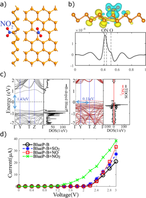
A major concern with chemiresistive and field-effect transistor (FET) based sensors is that the 2D transducer is directly exposed to air. Their ability to react with many ambient gases makes selectivity and specificity very difficult to engineer. We are currently investigating means to introduce selectivity to 2D materials through substitutional doping. When an atom of a 2D crystal is replaced by a noble metal, its characteristics can change towards the preferential adsorption of specific gas molecules. For example, we have shown that substitutional doping of blue phosphorene with boron atoms results in an improved selective sensitivity towards NO2, compared to NO and SO2, shown in Figure 1. 2D semiconductor based gas sensors also have great potential in integration with mature CMOS technology, as they can be introduced during back-end-of-line (BEOL) fabrication.
Integration of Semiconductor Metal Oxide Gas Sensors
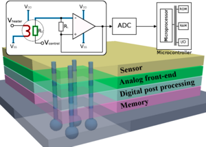
Because system-on-package suffers from long wires and high resistance-capacitance (RC) delay, the pinnacle of sensor integration is its fabrication within a CMOS sequence on a semiconductor substrate, commonly using three-dimensional (3D) integration, shown in Figure 2.
Currently, there are three main principles upon which solid-stage gas sensors are applied in large scale commercial use: Electrochemical sensors based on solid electrolytes, pellistors based on catalytic combustion, and semiconducting metal oxide (SMO) sensors based on conductometric or chemiresistive sensing. The SMO has the advantage of compatibility with CMOS fabrication and cost efficiency, which is why its use has prospered. Many other research activities for a variety of sensor technologies is ongoing including building automation, smart traffic, biosensing, spintronic materials, temperature sensors, and many others
The added benefits of SMO sensors is their high sensitivity to many polluting and toxic gases (VOCs, CO, CO2, CH3OH, NH3, H2S, and many more) at very low concentrations, with fast response times, ease of maintenance, low cost, and scalability towards their use in portable devices. One downside, however, is poor selectivity towards a target gas molecule since it is difficult to ascertain which specific molecule has caused a change in the surface charge density. In addition, the film must be heated to temperatures between 250°C and 500°C to ensure a surface reaction.
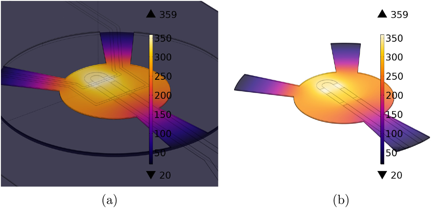
We study how temperature can be used to design low-power sensor arrays by introducing microheater arrays, which provide different target temperatures to different sections of the sensing film, tailoring them in this way towards a particular gas molecule. One of our achievements is the design and simulation of a low-power microheater array which simultaneously provides different temperatures from a single power source to several locations on the sensor membrane, shown in Figure 3. This allows for a significant reduction in power, enabling the potential application of this type of sensor in wearable electronics.