|
Today, state of the art Metal-Oxide-Semiconductor (MOS) devices have critical features in the sub 100nm range. This results in device regions, such as the channel in a MOS Field-Effect
Transistor (MOSFET), which only contains a few discrete dopands. MOS device characteristics, such as the threshold voltage, are thus already significantly influenced by even the
slightest deviations in size and dopant distribution among other influences, such as line edge roughness. These few randomly distributed dopands in the channel lead to the gate voltage
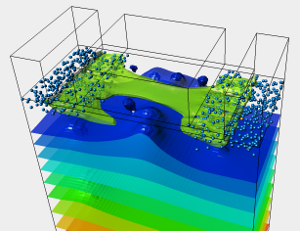
dependent formation of so-called current percolation paths in the channel of the MOSFET (cf. figure). Whenever a device is subject to a bias temperature stress for a sufficient amount
of time, oxide defects are formed directly above the channel where the current flows.
If such an oxide defect is placed directly above a current percolation path, the defect is likely to become charged and will block the current flow in the percolation path underneath.
This results in a sudden drop in drain current, which can cause the circuit that the MOSFET is operating in to fail. In order to assess such a worst case scenario and to make realistic
lifetime predictions for state of the art MOS devices, a statistically relevant number of microscopically different devices have to be measured and simulated. Comparison via
measurements and simulations have provided greater insight into the underlying physics, allowing for more accurate lifetime predictions.
Oxide defects in high voltage and scaled devices also play an important role in the description of Hot Carrier (HC) effects. In order to test our current models for hot carrier
degradation, self-consistent simulations of HC effects are necessary. For such simulations a replacement for the time consuming Monte Carlo simulator is currently under development,
using a spherical harmonics expansion of the Boltzmann transport equation, featuring models for important physical effects present in semiconductor devices, such as impact ionization
and electron-electron scattering.
|