|
GaN-based High Electron Mobility Transistors (HEMTs) attract strong attention due to their material relevant properties, such as wide bandgap, high carrier saturation velocity, thermal
conductivity, and high breakdown field, which are required for high-temperature, high-power, and high-speed applications.
We study InAlN/GaN HEMT structures both experimentally and by means of two-dimensional device simulations with Minimos-NT. The I-V measurements are performed using a highly accurate,
fully automated parameter analyzer. Very good agreement between measurements and simulations with Minimos-NT is achieved by using the hydrodynamic transport model and by including self-
heating and impact ionization effects. The simulations rely on a well-calibrated set of material-specific model parameters, which depend on temperature, carrier energy, etc.
Next to the DC device characteristics, the focus of our investigations is the HEMT off-state breakdown behavior. In our particular structure, the gate leakage current is almost invariant
to drain voltage. On the other hand, the source-drain leakage current increases steadily with drain voltage and significantly overpasses the gate leakage current when the hard breakdown
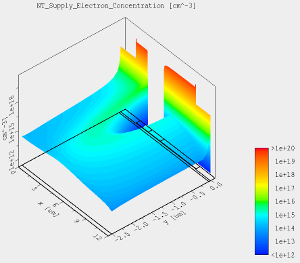
occurs. This behavior strongly indicates that the breakdown event is triggered in the buffer layer of the device. The simulated two-dimensional electron concentration map of the studied
HEMT in the pre-breakdown condition shows a significant penetration of the space charge region into the GaN buffer and its extension towards the drain. The peak electric field occurs at
the drain side of the gate. A significant increase of its magnitude up to 6MV/cm is observed, which might cause carrier avalanche multiplication in the channel. Parasitic conductivity in
the buffer layer, partly caused by the activation of the defect states, also restricts the
breakdown voltage, which in turn limits the design of transistors with smaller source-to-drain distances for high power applications.
|