|
Hot-Carrier Degradation (HCD) of a Metal-Oxide-Semiconductor Field-Effect Transistor (MOSFET) is conventionally associated with the build-up of interface states and oxide trapped
charges. Therefore, quantitative information on the defect spatial distributions is essential to reveal and understand the physical mechanisms of the HCD phenomenon. For this purpose,
the Charge-Pumping (CP) technique is widely used. Most methods for extraction of the lateral defect profiles from CP data employ a constant transistor oxide capacitance. In such an
approach the MOS structure is considered as an ideal infinite parallel-plate capacitor or, in other words, the oxide electric field is assumed to be uniform. However, accounting for the
fringing effect is of great importance for the characterization of the defect spatial distributions after hot-carrier stress because the interface state density peak is located near the
drain end of the gate where the electric field non-uniformity is most pronounced. Thus, a compact analytical model for simplification of the defect profile extraction technique is of
great importance. For the solution of this problem the conformal-mapping method is used, which is most helpful for the analysis of the fringing electric field under simple 2D boundary
conditions (see figure 1).
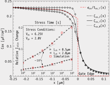
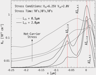
For characterization of the defect density evolution with the stress time the analytical local oxide capacitance distribution is incorporated into the conventional scheme. One can see
in figure 2 that the extracted defect profiles feature two peaks starting from 100s. Moreover, figure 2 demonstrates that these peaks just correspond to the maxima of the electron and
hole acceleration integrals. This result is confirmed by the findings of our HCD model, which shows that these peaks are related to the contributions induced by primary channel
electrons and secondary generated holes.
The obtained defect profiles were subjected to further validation as input parameters to simulate the linear drain current degradation. Comparison of simulated and experimental curves
once again confirms the applicability of the developed model (see figure 1, inset). It should be noted that the change of the linear drain current degradation slope appearing at 100s
for both devices can be linked to the contribution of the hole interface state density profile peak to the total defect density. This phenomenon will require further refinements in the
qualification procedure.
|