|
Silicon NanoWires (NWs) have attracted significant attention as efficient electronic and thermoelectric devices after the realization that length scale provides an additional degree of
freedom in engineering their electronic and thermal transport properties. Thermoelectric devices traditionally operate on low efficiency. However, nanostructured thermoelectric devices
with enhanced performance compared to their bulk counterparts have recently been realized. Silicon NWs with performance two orders of magnitude higher than that of bulk silicon have been
demonstrated. The thermoelectric performance of NWs can be further optimized by using the most beneficial transport and confinement orientations. In this way, the desired improved
properties of materials can be engineered to some degree.
We use the atomistic tight-binding sp3d5s*-SO model and Boltzmann transport equation with all relevant scattering mechanisms included, to investigate thermoelectric transport in silicon
NWs. We study the effect of physical quantization on the electronic structure of NW channels and identified the main electronic structure factors that influence their performance. It is
found that structural quantization below 10nm can severely affect the electronic properties of NW channels by changing the effective masses, changing the curvature of the bands, and
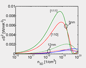
altering degeneracies through valley and subband splitting. Different wire orientations have different transport properties. Specifically for p-type NWs, it was found that at large
diameters, NWs oriented along the three principle orientations [100], [110] and [111], have a similar thermoelectric power factor. A large anisotropy in the thermoelectric power factor
was found, however, for smaller diameters. As the diameter is scaled to 3nm, the power factor of the [
111] and secondly the [110] NWs largely increases, whereas that of the [100] NWs remains low as shown in the figure. This behavior originates from confinement induced large curvature
variations in the subbands of these NWs. It demonstrates how the length scale degree of freedom can be utilized to improve the electronic and thermoelectric properties of nanoscale
devices. A similar behavior was observed for ultra-thin layers, in which case the power factor of the p-type (110)/[110] channel outperforms the power factor of all differently oriented
channels.
|