|
The reliability of interconnects in modern integrated circuits is determined by the magnitude and direction of the effective valence for ElectroMigration (EM). The effective valence
depends on local atomistic configurations. In order to study EM at an atomistic level, application of ab initio methods is necessary. EM experiments indicate that the copper interconnect
lifetime decreases with every new interconnect generation. In particular, fast diffusivity paths cause a significant variation in the interconnect performance and EM degradation. In order
to produce more reliable interconnects, the fast diffusivity paths must be addressed when introducing new designs and materials. The EM lifetime depends on a variation of material
properties at the microscopic and atomistic levels. Microscopic properties are grain boundaries and grains with their crystal orientation. Atomistic properties are configurations of atoms
at the grain boundaries, at the interfaces to the surrounding layers, and at the cross-section
between grain boundaries and interfaces. Modern Technology Computer-Aided Design (TCAD) tools, used in order to meet the challenges of contemporary interconnects, must cover two major
areas: physically based continuum-level modeling and first principles/atomistic-level modeling.
We investigate computationally efficient ab initio methods for calculation of the effective valence for EM and the atomistic EM force. The results of these ab initio calculations are
applied for parameterization of a continuum-level model and for simulation of the impact of the copper microstructure on the EM behavior. Additionally, an application of the kinetic Monte
Carlo method in combination with ab initio methods for EM study is utilized.
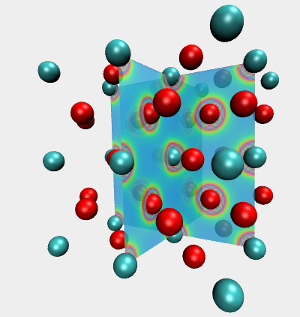
Several methods have been proposed for the calculation of the effective valence, all of them based on the computation of electron scattering states, such as the Density Functional Theory
(DFT), in connection with the Augmented Plane Wave (APW) method or the Korringa-Kohn-Rostoker (KKR) method. Since all of the previous methods demand cumbersome representation of
scattering wave functions with many parameters, which is a heavy burden on the stability and accuracy of subsequent numerical steps, we introduce and investigate new approaches, which are
based on orbital electron density.
|