|
Due to the continuous downsizing of Metal-Oxide-Semiconductor Field-Effect Transistors (MOSFETs), a keen interest has aroused in how the capture or the emission of single charges can
affect device reliability. In numerous publications, Random Telegraph Noise (RTN) in the drain current is unambiguously linked to the capture and emission processes (charge trapping).
Thereby, investigations based on time-dependent defect spectroscopy have provided deep insight into the microscopic physics behind these processes and have allowed a better understanding
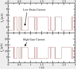
of current reliability issues, such as the Negative Bias Temperature Instability (NBTI). In a recent experimental publication, additional fluctuations of the gate current have been
observed and found to be occasionally correlated with fluctuations in the drain current (see figure 1), suggesting that a trapped charge somehow allows for Trap-Assisted Tunneling (TAT).
In literature, this tunneling mechanism is usually modeled as a sequence of two Nonradiative Multi-
Phonon (NMP) processes. Strikingly, such processes have already been used to explain reliability issues, such as NBTI.
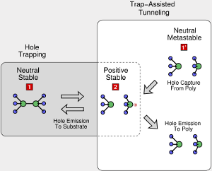
As a consequence, our previously suggested multi-state model for NBTI has been extended in order to account for the charge exchange with the gate. In this comprehensive model, the TAT
current consists of two consecutive steps – namely, hole capture from the substrate (from state 1' to state 2) followed by hole emission to the poly gate (from state 2 back to state
1'). As shown in figure 2, the resulting TAT current only occurs for the positive charge state of the defect and can be switched on by hole capture (from state 1 to state 2) or turned off
again via hole emission (from state 2 to state 1). Naturally, this model can be generalized as electron trapping. The field and temperature dependence of the TAT current contains valuable
information about the defect properties, such as the trap levels and the barrier heights of the NMP transitions, and thus will provide a more detailed description of the defect.
|