|
In integrated circuit development the reliability and performance of advanced devices is a priority. Certain device characteristics have to be satisfied, which are directly affected by
process variations. To study the impact of these variations on desired device properties, TCAD simulations with varying process parameters were performed. N- and p-MOS transistors, each
with different geometries of an already established high-voltage LDMOS process, have been chosen as the basis for comparison.
Critical process parameters were selected as input for the process simulation. Their variation ranges were defined according to measurements that compared the validity of the achieved
results. To match the simulation with the measurements, characteristic parameters of the devices were extracted. Additionally, the same exact methodology that was used for device
characterization in production was adapted to the device simulation.
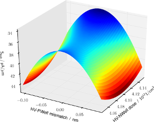
To overcome the extensive simulation time a minimum set of required input parameters, which consisted of three simulation levels in each parameter and a Central Composite Face-centered
(CCF) design, was chosen. When conducting a comparison with the measurements, only output parameters are visible. The originating input values are not accessible, therefore a comparison
with measurements has to be performed on the output values only. However, the resulting parameter distributions do not show the expected results compared to measurements. To achieve a
reliable comparison, the simulation results have been analytically modeled with a quadratic model of the input parameters by a least-square fit. Now this model is applied to randomly
distributed input parameters that show the same variation as parameters characterized from measurements. The output of this model now delivers a comparable sketch of parameter
distributions. Equipped with this set of input data, dependency model, and output data, further data analysis,
such as selectivity analysis or a continuative examination by SPICE models, can be performed.
|