|
The Level Set simulator for moving boundary problems has already been developed at this institute. The simulator uses Level Sets in order to identify and advance silicon wafer surfaces
and interfaces between different materials on a silicon chip for various physical processes. Nanolithography using Non-Contact Mode Atomic Force Microscopy (NCM-AFM) is a promising method
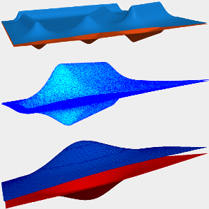
for the manufacture of nanoscale devices. Compact models, which suggest patterned oxide dots and wires with Gaussian or Lorentzian profiles, are implemented in the Level Set simulator. An
alternative to compact models is explored with a physics based Monte Carlo model, where the AFM tip is treated as a point charge and the silicon wafer as an infinite conducting plane. The
strength of the generated electric field creates oxyions, which accelerate towards the silicon surface and cause oxide growth and surface deformations. A physics based model is developed,
generating dots and wires based on the induced surface charge density. Comparisons to
empirical models suggest that a Lorentzian profile is better suited to describe surface deformations when compared to the Gaussian profile. Simulating a three-dimensional AFM problem
using a Lorentzian model requires a two-dimensional Lorentzian particle distribution around the AFM needle tip. A successful algorithm for a two-dimensional Lorentzian distribution was
found by integrating the probability distribution, while taking two-dimensional slabs of the surface into consideration. A second evenly distributed value is used to generate a radial
distribution. The resulting location of each particle can then be obtained, resulting in a physical representation of a NCM-AFM generated nanodot or nanowire.
The possibility of using the Level Set simulator for spray pyrolysis deposition was also explored. Spray pyrolysis is a process by which a thin film is deposited by spraying a solution
onto a heated surface. In order to simulate such a process, large aspect ratios need to be considered; the solution droplets travel relatively large distances (~10-50cm) compared to the
nanometer scale of the wafer geometry. The ambience must also be divided into two sections: one where the droplets travel unaffected by the thermal gradient and a second where the
increased temperature and thermal gradient play a major role in droplet movement as well as the location of each single particle deposition. The Monte Carlo method is used to simulate the
movement of the droplet and particles in the ambience, while a Chemical Vapor Deposition (CVD) model is used to simulate the interaction between the droplet and the wafer surface.
|