


Device Reliability
Textbooks typically deal with idealized devices. Real devices, however, contain defects which distort the device's characteristics. In mainstream silicon technologies, these defects are primarily located at material interfaces, for example at the Si/SiO2 interface between the insulating layer and the silicon channel in MOSFETs, as well as in the insulating material itself (SiO2, SiON, high-k). In addition to active defects, numerous defect precursor sites exist which can be converted into electrically active defects during device operation, for example through their interaction with highly energetic carriers or hydrogeneous species (H, H2, H2O, etc.).
Unlike silicon technologies, alternative channel materials also come with numerous defects in the semiconducting materials themselves, for example as in wide bandgap materials such as SiC or GaN or in the currentlyhighly popular 2D materials.
Hysteresis
Often in non-mainstream silicon technologies, the defect densities are typically so large that their impact is already apparent during the measurement of ID-VG characteristics via the emergence of a hysteresis of the current, that is, a different ID during up- and down-sweeps of VG. This phenomenon is seen in virtually all alternative technologies and is typically due to the charging of defects during the up-sweep. The emission times of some defects are too slow to allow for a discharge during the down-sweep, resulting in shifted ID-VG characteristics. Exploration of the hysteresis for various material systems reveals a lot of information on the contributing defects and is one of our research areas.
Noise
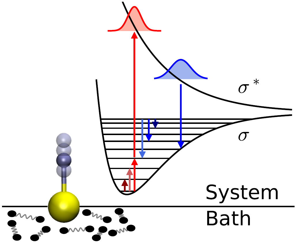
Similarly to hysteresis, noise in MOS structures is dominated by defects in the insulating materials. Given their broad distribution of time constants, experimental characterization is challenging. In large-area devices, noise is typically of a 1/f form (flicker noise), while in nanoscaled devices random telegraph noise (RTN) becomes visible. The superposition of a large number of RTN-causing defects is typically assumed to be responsible for 1/f noise. This connection, as well as the link between RTN and BTI (see below), provides another fascinating area of research.
Bias Temperature Instabilities
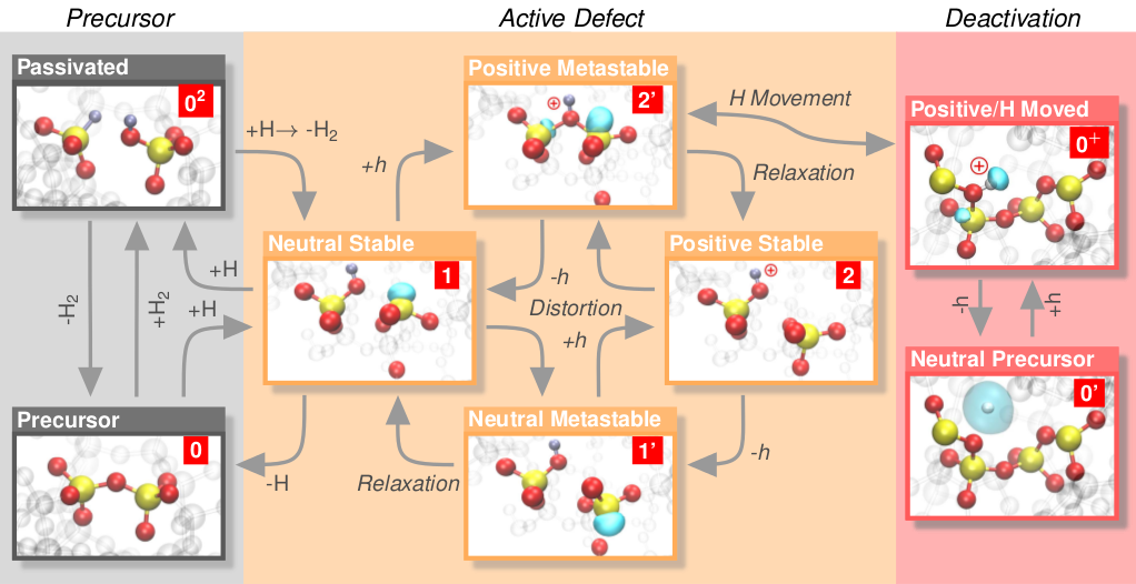
With continuing device operation, preexisting defects in the insulating material become charged. Since the time constants involved in these charging and discharging processes are typically widely distributed - ranging from sub-microseconds to weeks, months, and years -this effect results in slow drifts of the device characteristics, This is typically referred to as bias temperature instabilities (BTI), since the effect is significantly enhanced at higher temperatures. In addition to the charging of preexisting defects, new defects can be created, very likely due to interactions with hydrogeneous species released during the charging process. Many open questions exists (particularly regarding long-term degradation) and are currently under investigation.
Hot Carrier Degradation
As soon as a larger drain voltage is applied, carriers can pick up energy while they traverse the channel. The energy distribution is strongly influenced by scattering mechanisms such as impact ionization and particle-particle scattering. For an accurate description, the solution of the Boltzmann transport equation is typically required. The precise nature of the interplay between these energetically distributed carriers and defects (typically passivated bonds at the interface or oxide defects) is currently a "hot" topic of research in our group.
Experimental Characterization
Reliability modeling relies heavily on a precise characterization of the time-dependent degradation. Given the broad distribution of time constants or reaction rates (from sub-microseconds to weeks, months and years, depending on the temperature), highly specialized equipment and know how is required, see here.