AI for Microelectronics
Artificial Intelligence (AI) is becoming an indispensable tool in microelectronics research, helping address challenges ranging from atomistic materials modeling to large-scale equipment simulation. In our work, we develop and apply physics-informed machine learning (ML) methods to accelerate simulations, improve model accuracy, and enable inverse design across all scales of semiconductor fabrication.
Machine Learning Interatomic Potentials (ML-IAPs)
Machine-learned interatomic potentials (ML-IAPs) are transforming atomistic modeling by extending the accuracy of first-principles methods like Density Functional Theory (DFT) to larger systems and longer time scales. These potentials are trained on ab initio datasets and retain quantum-level fidelity while enabling simulations that are orders of magnitude faster, making them ideal for investigating materials beyond the limits of traditional atomistic techniques.
In our research, ML-IAPs serve as a general-purpose framework to study a wide range of materials phenomena, both within and beyond microelectronics. Key applications include:
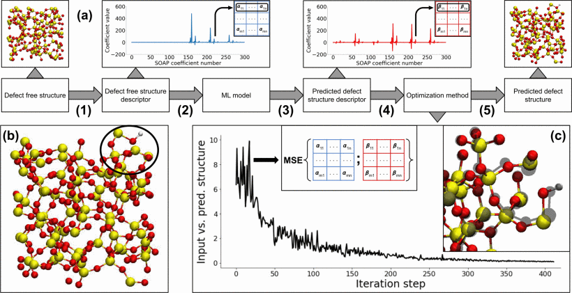
- Defect structure prediction and classification in amorphous and crystalline materials (e.g., a-SiO2, MoS2), using local atomic descriptors and unsupervised learning methods, as illustrated in Fig. 1.
- Ion-surface interactions, such as predicting etching and sputtering yields during plasma processing, where ML-IAPs capture the complex response of surfaces to energetic particle bombardment.
- Doping and activation processes in wide-bandgap semiconductors like SiC and GaN, where ML-based simulations help reveal defect energetics, implantation damage recovery, and thermal annealing pathways.
- Mechanical and thermal property evaluation of emerging materials, including the role of defects, surfaces, and interfaces under stress or irradiation.
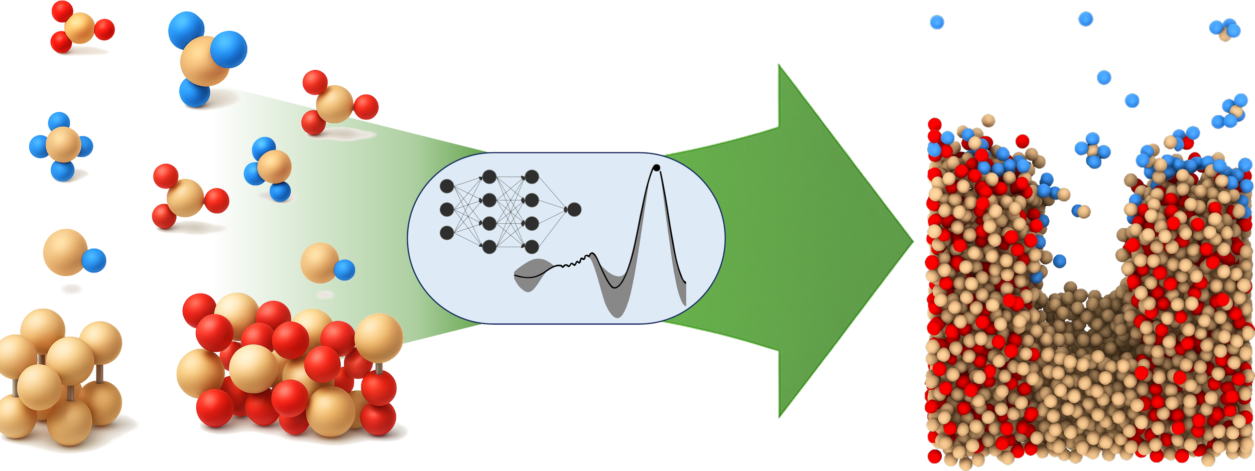
These ML-driven atomistic tools form a foundational part of our multi-scale modeling infrastructure, enabling predictive insights into material behavior that feed directly into higher-level device and process simulations. ML-IAPs are especially valuable in the context of semiconductor reliability, advanced fabrication methods, and new material exploration. This capability allows us to increase the useful time and length scales of molecular dynamics (MD) simulations without any loss in accuracy. For example, we can study atomic-layer silicon etching with fluorine radicals, where direct DFT-based molecular dynamics would be prohibitively expensive. As shown in Fig. 2, small-scale DFT calculations capturing elementary surface reactions are used to train ML potentials, which then drive large-scale molecular dynamics simulations of etching processes with full atomic detail.
Surrogate Models for Equipment-Level Simulation
On the fabrication side, microelectronics process simulation increasingly relies on bridging scales: From full reactor modeling down to feature-scale predictions. However, direct simulation of plasma reactors using fluid-kinetic or hybrid models remains computationally expensive and is impractical for rapid parameter sweeps, optimization, or inverse design tasks.
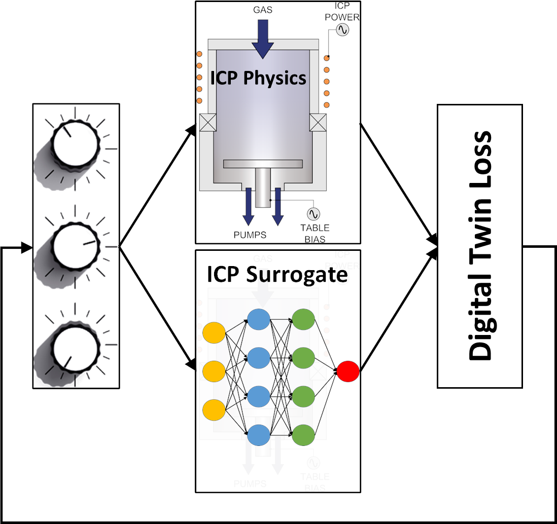
To overcome this limitation, we develop surrogate models, also referred to as digital twins, that emulate the input-output behavior of full reactor simulations. These surrogates are trained on high-fidelity simulation or experimental data and provide fast, differentiable approximations of boundary fluxes (e.g., ion and neutral distributions) as functions of process parameters like coil power, gas composition, chamber pressure, and bias voltage. The training workflow is illustrated in Fig. 3, where a neural network is optimized to reproduce the outputs of a full inductively coupled plasma (ICP) simulation. The surrogate learns the reactor’s response to different control knob settings, minimizing the deviation from the physics-based simulation through a defined loss function.
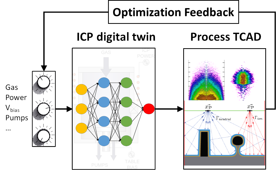
Once trained, the surrogate can be deployed in inverse modeling and feedback workflows. As shown in Fig. 4, the digital twin is embedded in an optimization loop that tunes reactor parameters to achieve desired outcomes at the feature scale, such as specific ion angular distributions or etching profiles, predicted using feature-scale TCAD tools like ViennaPS. This approach enables real-time process optimization and design-space exploration, significantly accelerating the traditionally slow and sequential calibration cycle.
This framework enables physics-informed learning and interpretable surrogate modeling, tailored to the needs of semiconductor process optimization. By integrating global sensitivity analysis and explainable ML techniques, such as SHAP values and Sobol indices, we can identify dominant process parameters, uncover cause-effect relationships within the reactor, and support the development of intelligent control strategies and digital fabrication twins.