


Technology Characterization Laboratory
The Technology Characterization Laboratory (TCL) at the Institute for Microelectronics was founded in 2012. Since then, the laboratory has been consistently extended to meet the changing requirements of characterization challenges which are essential to conduct device research beyond state-of-the-art. This is achieved by conducting experiments mainly aimed at the electrical characterization of modern transistor structures. The principal focus of our experiments is devoted to defect spectroscopy in semiconductor transistors. Within this field n-channel and p-channel MOS transistors employing SiO2, SiON, or high-k materials as gate insulator are thoroughly analyzed. Furthermore, transistors using more exotic materials based on 2D materials (Graphene, MoS2, etc.) or lateral and trench MOS transistors, fabricated on silicon-carbide, substrates are also being investigated.
For the characterization we apply conventional measurement techniques such as ID-VG and hysteresis measurements and C(V) measurements. To analyze the impact of stress on the device characteristics, measure-stress-measure (MSM) schemes are used. We also conduct combined C(V)-stress-C(V) sequences to evaluated small changes in the device electrostatics when stress conditions are applied. The long list of additional measurement options is consistently extended and individually adapted to the growing challenges. To perform the experiments our laboratory facilities comprises general purpose and custom-made measurement instruments.
The tremendous advantage of our equipment is that it can be individually adapted to suit the most complex measurement requirements. This enables us to get an in-depth understanding of fundamental physical processes in the components and successfully contribute to further improve them. We are very encouraged to discover new interesting technologies.
Defect Probing Instrument (DPI)
Our DPI is especially targeted to apply single defect spectroscopy in nanoscale MOS transistors but is also suitable to characterize large area devices.
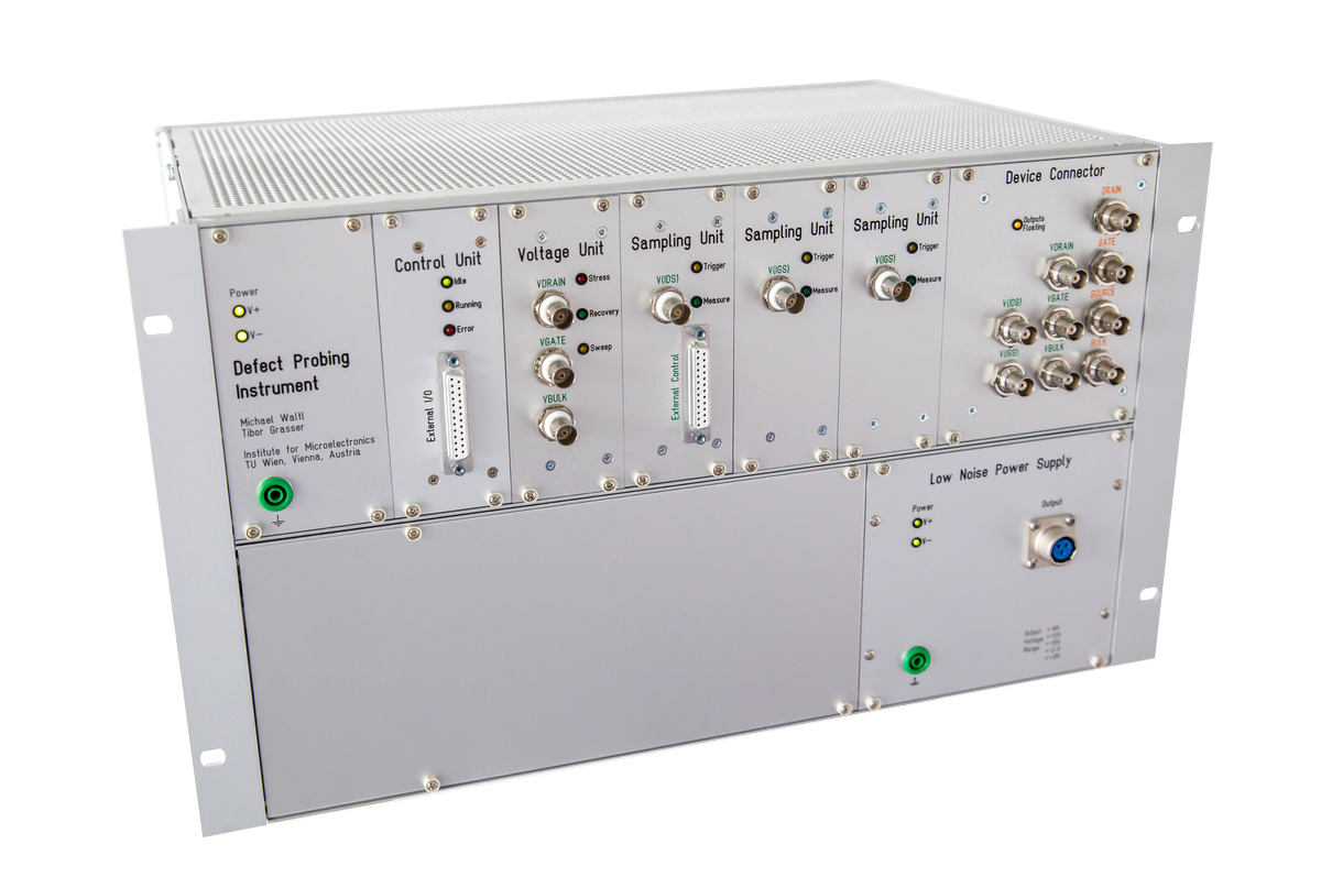
The high measurement resolution in the sub-picoampere regime and at sampling rates of up to 1MHz is essential for fast the characterization of oxide and interface traps. Furthermore, the DPI can be permanently operated using battery power enabling measurements at the lowest possible noise level. Another significant advantage of the DPI is application-specific programmability and configurability; for instance, MSM sequences and C(V) measurements can be performed without changing any electrical connections. Furthermore, the experiments are highly stable and measure sequences can be run for more than a year without an interrupt.
General Purpose Instruments (GPI)
The GPIs, available in our TCL, comprises instruments developed from Keithley and Jäger Messtechnik. We use the Keithley 2602A and 2636A source-measure-units to conduct experiments with biases up to 200V and a current resolution down to a femtoampere. Additionally, an ADWin setup is available to implement individual measurement sequences.
In order to successfully carry out experiments, contacts to the test devices must be provided. For this purpose, depending on the temperature range, sample size (small silicon chips or entire wafers), ambient conditions (vacuum or air), and expected net measurement time on a single device (few microseconds or several months) a variety of modern equipment is available in our TCL.
Cryogenic Probe Stations (CPSs)
Usually the superposition of many different physical effects appearing at the same time is measured.
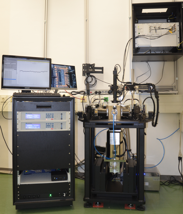
However, it may possible to disable thermally activated physical processes at cryogenic temperatures. Furthermore, a reduction of the ambient temperature might allow for a probing of electrical effects with time constants which are incapable of measurement at room temperature. Using liquid nitrogen or liquid helium, our cryogenic CPSs enable low temperature measurements down to 4.2K under high vacuum (typically 10-6Torr). The high temperature limit is 650K. To contact the samples the CPSs provide six electrical probes. An optical probe enables optical excitations to be applied to the sample.
Semiautomatic Probe Stations (SPSs)
SPSs are convenient any time extensive statistic collection over many devices is required. Our PA300 is capable to automatically contact devices on wafers with diameters up to 12in and can heat the devices up to 200°C. Additionally a SPS for wafers up to 8in diameter is available.
Furnace Setups (FS)
The need to characterize devices under stable temperatures without any interrupt for a long time is met using specialized furnaces operated in our TCL. To ensure low contact resistance, but at the same time guarantee highly stable contacts the silicon chips are typically glued and bonded into ceramic packages. The FS are targeted to load DIL24 packages. To guarantee the long-term stability and fail-safe operation, additional uninterruptable power supplies are used. The measurement itself is performed using our DPI.
Long-Term Defect Prober (LTDP)
Our TCL also provides custom-made LTDPs using up to eight micromanipulators to directly contact samples on semiconductor chips with an area up to 1in2. Alternatively, the LTDPs are also suitable for probe-cards enabling the measuring of several transistors in parallel. The heater used is typically capable to heat the silicon chip up to 250°C. To conduct the electrical measurements the DPI is commonly used, but also the GPI can be connected to the LTDPs.
Additional Equipment
Other custom-based solution use for instance metal-ceramic-heaters in combination with a dedicated temperature controller to stress or anneal samples at temperatures up to 600°C.