In the first part of this chapter, charge trapping at the surface of GaN/AlGaN HEMTs at different forward bias stress conditions is investigated. It will be shown that in order to correctly model the observed charge trapping, the electrostatic feedback of the charges has to be taken into account by using self-consistent transient simulations. In particular the stress history of the device and local potential changes lead to different dynamics of each individual defect.
In the second part, a single defect characterization on complex three-level RTN measured at cryogenic temperatures on nanoscale GaN/AlGaN fin-MIS-HEMTs will be carried out. First, the energy levels and vertical positions of the defects are extracted using a simple two-state model together with TCAD simulations and the spectral method explained in Section 6.6.3. In the following, the hypothesis of having two coupled two-state defects is questioned by estimating the required coupling factors and comparing them to values acquired by different methods. Based on these findings, two different defect candidates are chosen and investigated using HMM training as put forward in Section 6.7.
Threshold voltage drift, especially at forward gate bias, is one of the major reliability issues for GaN/AlGaN MIS-HEMTs [75, 94, 189, 190]. Measurement studies revealed broad distributions of capture and emission times for the defects present at the interface between AlGaN barrier and insulator. In addition, several studies point out that transport through the barrier layer can have a significant influence on the recovery dynamics of these devices [AGJ1][93]. Additionally, the huge surface defect densities of about 1 × 10¹³/cm2 present at the insulator interface pose a challenge to their experimental characterization [AGJ8][75]. The observed threshold voltage shifts can thereby even approach the theoretical limit of charge storage in a double capacitor model for different insulating materials [66]. Another consequence of the large defect densities together with the depleted barrier region at recovery conditions is that the influence of charge feedback on the surface potential is much larger when compared to silicon technologies [191].
The following sections are dedicated to a simulation study on the forward gate bias  drift using the NMP charge trapping model with a special focus on the impact of charge feedback on the recovery kinetics of the device [AGC1].
The investigated devices were formed on a 1 µm GaN buffer grown on a silicon substrate with a 10 nm thick  barrier on top. The gate length was 1 µm, insulated from the barrier with a 25 nm thick SiN layer. In order to save computation time, the source and drain regions as well as the access regions were scaled to 500 nm. The substrate material was replaced by an aluminum
contact because in the investigated bias regions, the bulk region is effectively screened by the electrons in the 2DEG. The simplified device geometry used in the simulations can be seen in Figure 7.1. All
simulations were conducted using the device simulator Minimos-NT [21].
barrier on top. The gate length was 1 µm, insulated from the barrier with a 25 nm thick SiN layer. In order to save computation time, the source and drain regions as well as the access regions were scaled to 500 nm. The substrate material was replaced by an aluminum
contact because in the investigated bias regions, the bulk region is effectively screened by the electrons in the 2DEG. The simplified device geometry used in the simulations can be seen in Figure 7.1. All
simulations were conducted using the device simulator Minimos-NT [21].

barrier is placed on top of a 1 µm thick GaN layer. The thickness of the SiN gate dielectric is 25 nm with a gate length of 1 µm. To obtain reasonable simulation times, the access regions as well as the source and drain lengths are scaled to 500 nm each.
All metal contacts are formed using aluminum (from [AGC1]).
The net polarization charges at the interfaces are calculated with the data provided by Ambacher et al. [192]. The polarization charges at the interface to the substrate are considered to be fully compensated within the highly-defective transition region between the silicon substrate and the GaN buffer. The net charges at the barrier-buffer interface are simply given by the difference between the spontaneous polarization in the buffer and the spontaneous and piezoelectric polarization in the barrier layer. The interface between barrier and dielectric is somewhat more complicated since according to the surface donor model, the negative polarization charges at that interface are compensated partly or fully by positive defects. Additional information on the polarization charges in GaN based devices and the formation of the 2DEG can be found in Sections 2.2.4 and 2.3.1.
According to [192], the polarization charges can be calculated as:
The sheet carrier density at the channel interface is simply the difference between the polarizations between barrier and buffer layer.
Up to date there is no solid experimental evidence on the exact defect density of the surface donors [AGJ8][66]. Nonetheless, the sheet carrier density
serves as a lower limit to the number of positive charges present in the device due to charge neutrality requirements. Theoretically, all of the charge caused by spontaneous and piezoelectric polarization in the  layer needs to be compensated by defects at the surface, which is approximately three times as large as the sheet carrier density in the channel.
This could also serve as a possible explanation for defect densities larger than the sheet carrier density of the device ( ) observed at the insulator interface of different GaN based MIS-HEMTs [66]. Independently of the charge captured by defects at this interface, the number of positive compensation charges and thus the net amount of
polarization charges can also be estimated by comparing the threshold voltages of devices from the same technology but with different dielectric thicknesses. In thermal equilibrium, the barrier layer of the MIS-HEMT is depleted by the polarization field and thus effectively acts as a capacitor.
) observed at the insulator interface of different GaN based MIS-HEMTs [66]. Independently of the charge captured by defects at this interface, the number of positive compensation charges and thus the net amount of
polarization charges can also be estimated by comparing the threshold voltages of devices from the same technology but with different dielectric thicknesses. In thermal equilibrium, the barrier layer of the MIS-HEMT is depleted by the polarization field and thus effectively acts as a capacitor.
Because of the fact that only the dielectric thickness changes on top of the same layers, the net positive charge at the dielectric interface defines the threshold voltage of the device. Under the assumption of the barrier layer acting as an ideal capacitor, the voltage divider between the gate dielectric and the barrier can
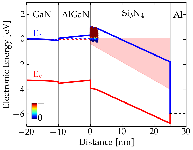
be used to calculate these charges (see Figure 7.2). In the picture, is shown for different fractions of the theoretical polarization charges being compensated by positive surface donors. It can be seen that the best agreement is obtained for 95 % of the piezoelectric charges being compensated.

is shown for different amounts of (negative) polarization charges being compensated by positive surface donors. The best agreement is obtained for 95 % of the piezoelectric charges being compensated (reprinted from [AGC1]).
In the simulations, deep donor traps were placed into the buffer and barrier layers at an energy level of about 0.6 eV below the GaN conduction band with concentrations of 1 × 10¹⁶/cm3 and 5 × 10¹⁶/cm3 respectively. The energy levels were chosen
according to the most common defect levels present in GaN, see Figures 3.1 and 3.2. To
describe the transport of carriers from the channel to the barrier, a thermionic field emission model is employed [193]. The band alignments between the buffer, barrier and SiN layers as well as the workfunction difference of  for the aluminum gate are set using the data provided by [194].
As the majority of electrically active defects are thought to be at the dielectric interface of the device, the NMP traps are placed evenly within the first 2 nm of the SiN layer. Their concentration is calculated based upon the results from Figure 7.2. Figure 7.3 shows the distribution of defects in thermal equilibrium along a vertical cut through the gate of the device together with the band energy profiles. The shaded area depicts the active energy area between a gate stress bias of 4 V and a gate recovery bias of 0 V. In general, the active energy area is defined as the region between the Fermi levels of gate and barrier interface for a certain stress and recovery bias. Within this region NMP defects are able to capture and emit electrons during stress and recovery respectively. The charge state of each NMP defect is depicted by its color, red for positively charged defects and blue for neutral ones. As the results depict the thermal equilibrium of the device, they do not take into account the transient effects discussed in the following sections.
In order to calibrate the NMP defect model as well as possible, the transient simulations need to follow the experimental procedure provided in [75, 190] as close as possible. The data was recorded by an eMSM setup where the measurements are conducted for a variety of different stress times and forward bias voltages. A discussion of the eMSM measurement procedure together with typical bias conditions can be found in Section 4.1.3.
Since barrier related effects like the transport of carriers to the dielectric interface and its contribution to the measured time constants are still barely understood, the study was focused on stress voltages above the spillover region. In this region, a second electron channel is formed at the barrier/dielectric interface due to the high forward gate bias. This rules out any barrier transport effects for charge capture because the supply of trapped carriers will preferentially be provided by this second channel.
In the case of recovery, the situation can be different, since the captured electrons need to be transported through the barrier after emission from the defect. Reverse leakage studies on Schottky devices often suggest Fowler-Nordheim tunneling [141] for low temperatures and high reverse bias conditions and Frenkel-Poole like trap-assisted tunneling [152] for high temperatures and low reverse bias conditions respectively [41, 42]. A study on the onset of drift recovery at different voltages and temperatures extracted an apparent activation energy of 0.65 eV for barrier transport, slightly decreasing for lower positive voltages (i.e. high barrier fields)[AGJ1]. That value approximately matches the surface potential of the fully processed SiN devices at thermal equilibrium extracted from the simulations. These findings support the hypothesis of a transport mechanism via the AlGaN conduction band, most likely a thermal emission or field-enhanced thermal emission of carriers from the defects to the conduction band. Once in the conduction band, the carriers are transported towards the channel through the barrier field. Both effects are covered by the TCAD simulations and therefore should not have a significant influence on the extracted defect parameters.
The observed recovery behavior in these devices can be modeled with two sets of NMP defects with normally-distributed parameters, one for the more permanent part of the degradation and one for the more recoverable part. With the same set of defects, excellent agreement is reached for eight orders of magnitude in stress time and for three different stress voltages. The measurements together with the simulated recovery traces are shown in Figure 7.4. Even for the worst case stress conditions (10 V/10 s), the largest observed degradation only corresponds to a trap occupancy of approximately 25 %. Note that the used defect density in the simulations is still a lower bound to the real situation as only the amount of donor-like traps calculated from Figure 7.2 are considered. Defects with acceptor-like behavior and possible amphoteric states of the donor-like defects within the bandgap are not covered by the simulations either.
Significant deviations from the measurements are only found for large stress times and short recovery times up to about 1 ms. This can most likely be explained by a lack of fast NMP defects being within the active energy area at the specific stress voltage in the simulations. This can be either attributed to a lack of variance in defect distributions or to the fact that the simulations were carried out using the band edge approximation, where the NMP model only considers the conduction band minimum and valence band maximum instead of the continuum of states in the respective bands of the barrier. On top of that, other transport mechanisms through the barrier not covered by the thermionic emission model like trap-assisted tunneling or Frenkel-Poole conduction could potentially lead to faster effective emission times of the bound electrons especially at elevated stress times.
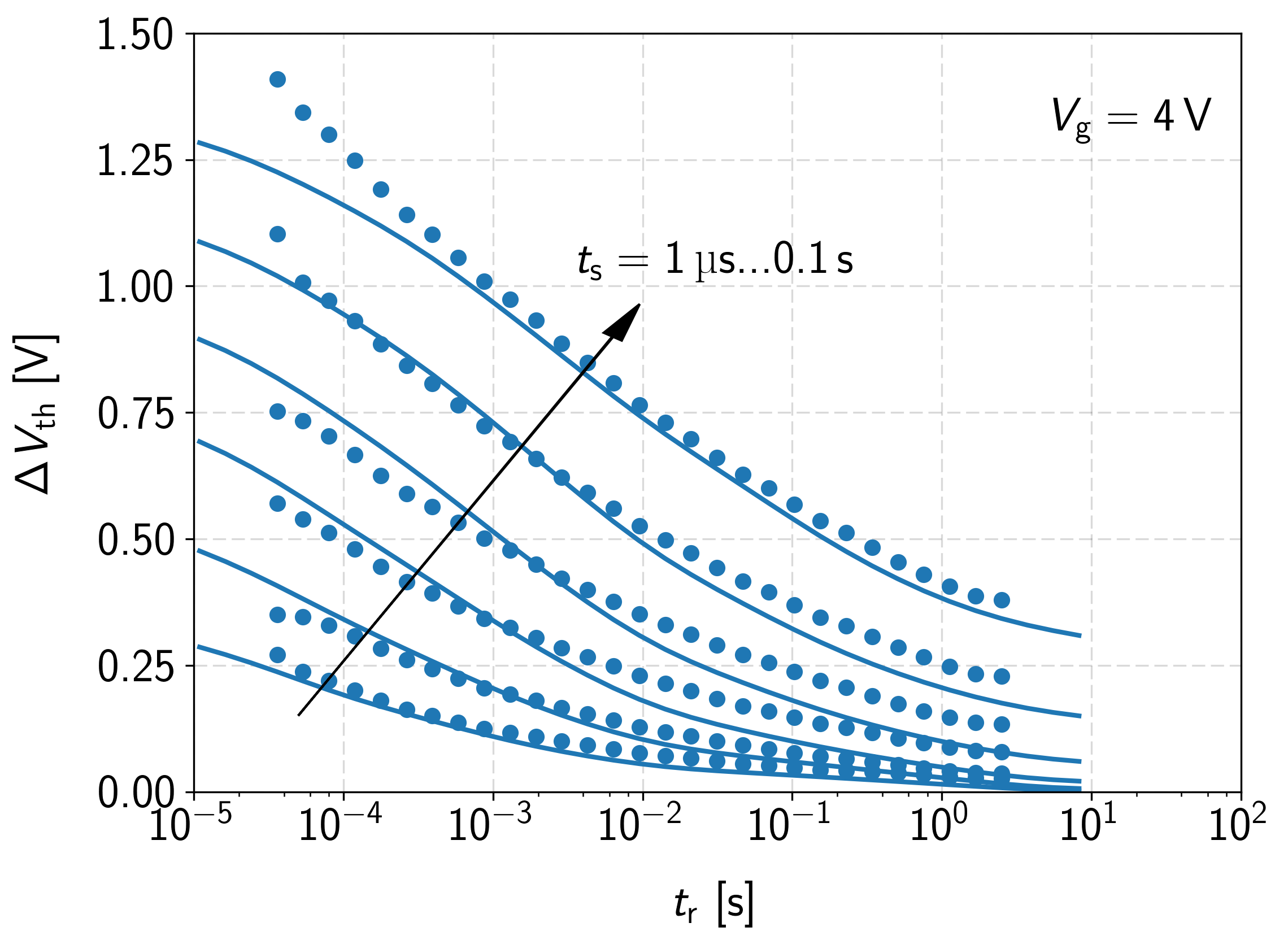
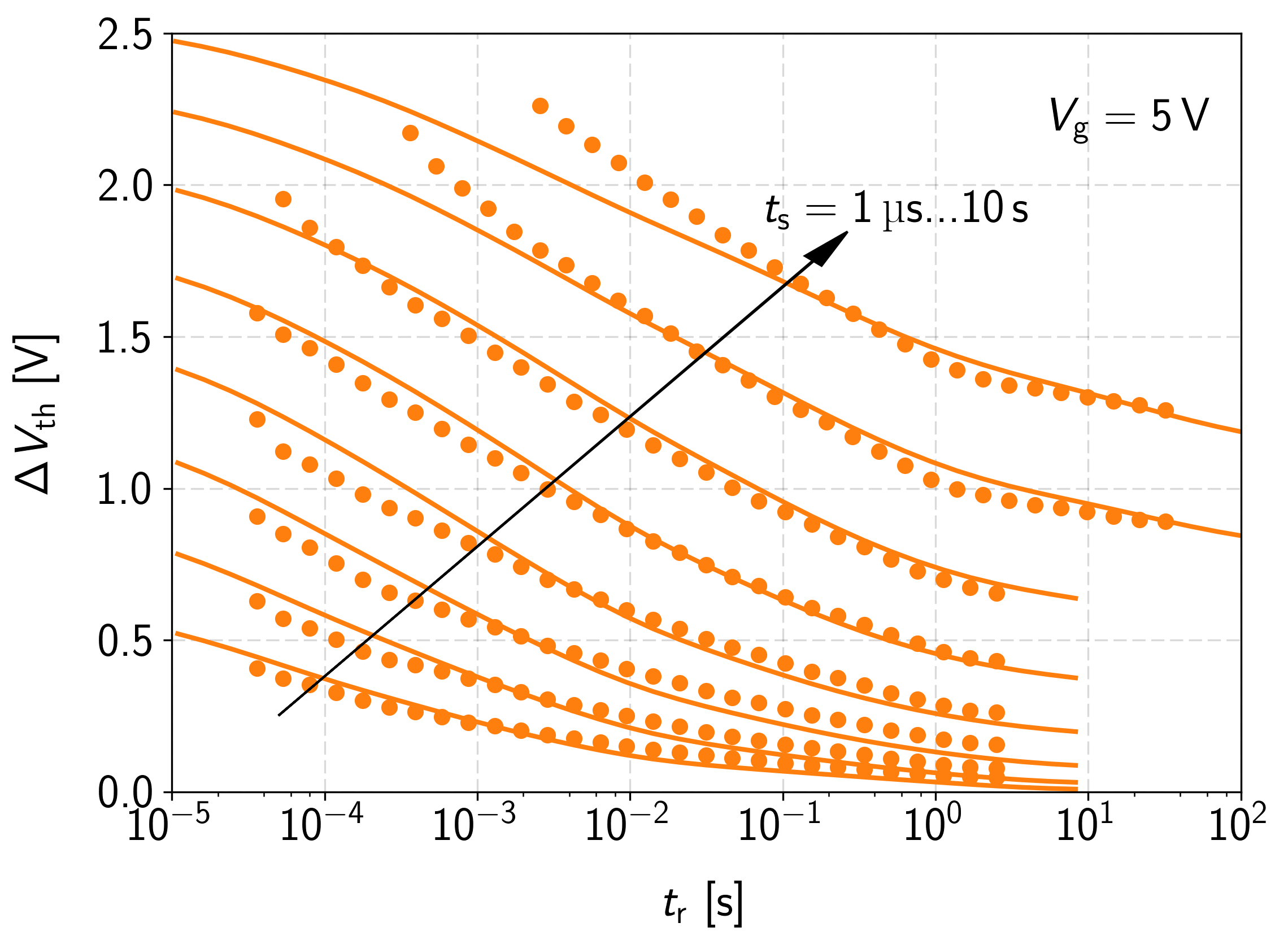
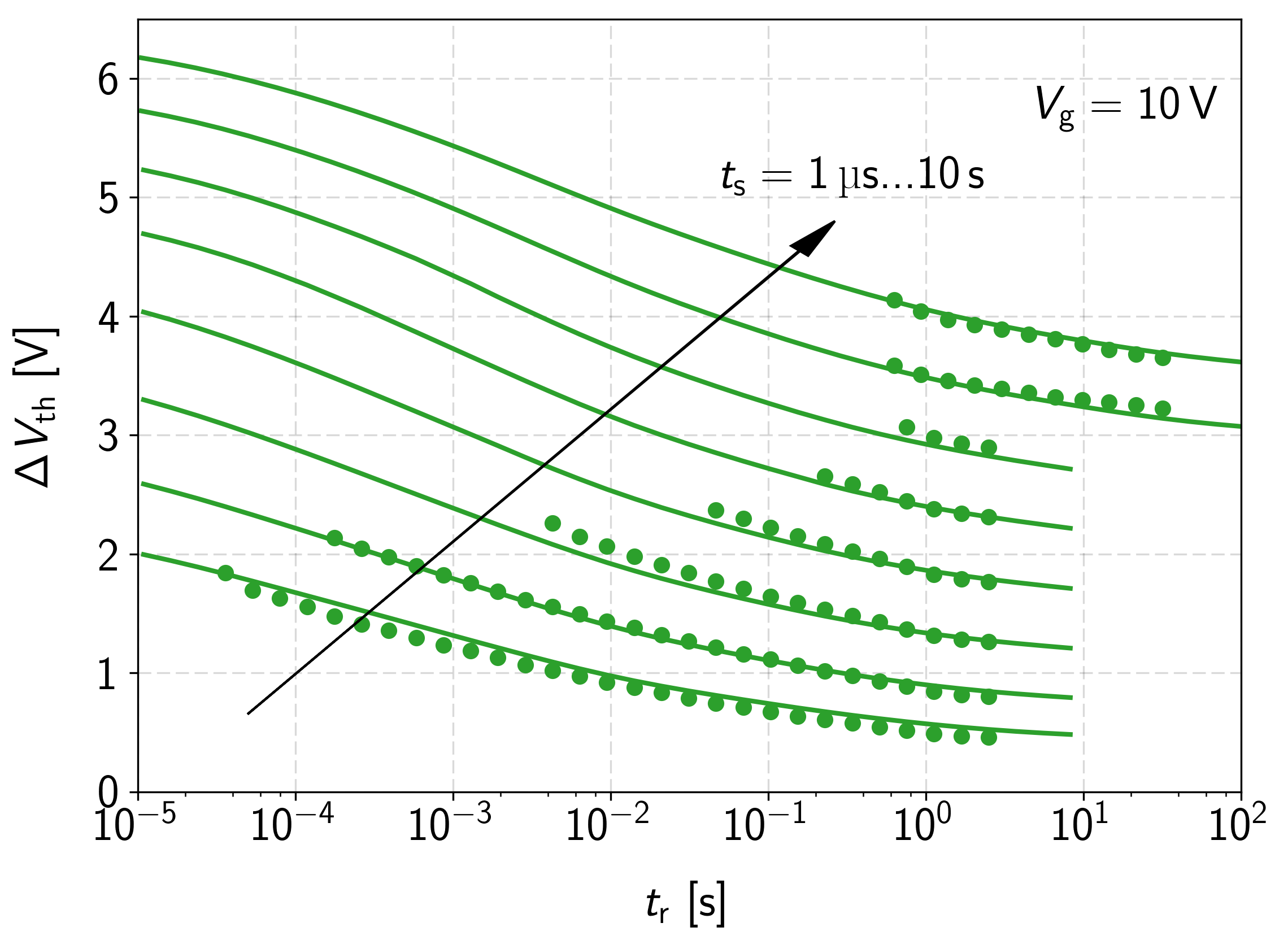
 recovery traces for eMSM sequences with stress times up to 10 s at room temperature. With two sets of normally-distributed NMP defects, the recovery behavior can be modeled for three different stress voltages of 4 V (blue), 5 V (orange) and 10 V (green) (reprinted
from [AGC1]).
recovery traces for eMSM sequences with stress times up to 10 s at room temperature. With two sets of normally-distributed NMP defects, the recovery behavior can be modeled for three different stress voltages of 4 V (blue), 5 V (orange) and 10 V (green) (reprinted
from [AGC1]).
Due to the large defect densities observed in all BTI experiments in GaN/AlGaN MIS-HEMTs, the question arises to what extent the response of these trapped charges has an influence on the recovery behavior of the device. This is of special interest if the nature of the surface donors should be revealed in the future. Various feedback mechanisms like local interactions or temporal changes in the surface potential due to the electrostatic feedback of the defects can potentially obfuscate the extracted defect parameters if not taken properly into account.
In contrast to silicon technologies, where at typical BTI recovery conditions a medium to strong electron channel is present at the dielectric interface, the situation in GaN/AlGaN MIS-HEMTs is different. Even if the device is still turned on at recovery, the barrier layer separates the dielectric interface from the electron channel. The polarization induced field causes a fully depleted barrier layer even for recovery voltages around 0 V (even more so for more negative gate voltages). In the case of silicon, the surface potential during recovery is pinned by the electron channel and thus its sensitivity on charge trapping is usually negligible. On the other hand, in GaN devices the depleted barrier layer causes a strong sensitivity of the surface potential on charge trapping.
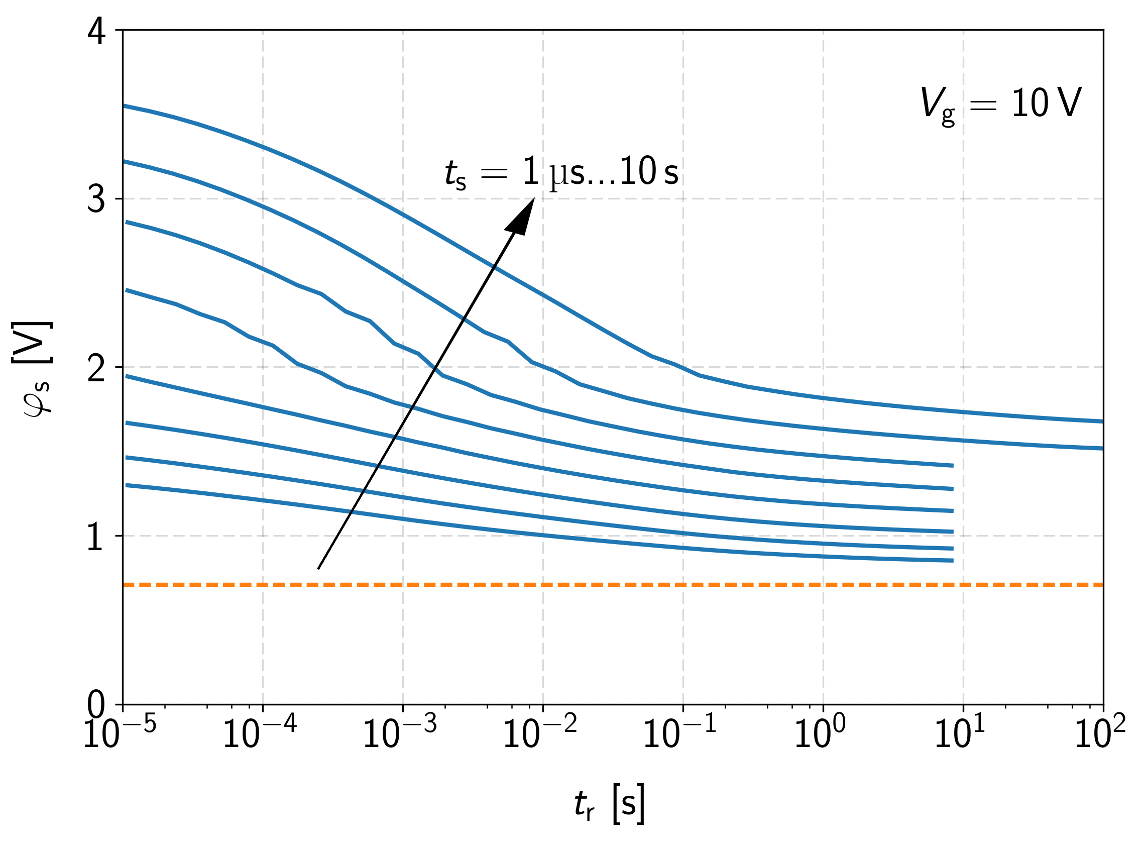
Electrostatic charge feedback (i.e, the change of the surface potential due to charge trapping) is even more amplified because of a large number of charges trapped at the dielectric interface as compared to BTI in silicon devices. The impact of drift on the surface potential for a stress bias of 10 V is depicted in Figure 7.5. For long stress times, the values can be up to 3 V larger when compared to the equilibrium value
(dashed line). Naturally, this effect has a significant impact on the drift characteristics.
On one hand, the trap levels of the defects close to the interface will experience approximately the same amount of shift as the potential at the interface. Since that shift enters the capture and emission times exponentially, the recovery times of all defects will show a strong transient behavior following the partial
recovery in the surface potential shift. On the other hand, the active energy area of the defects will also be a strong function of the trap occupancies, causing atypical phenomena like charge capture during recovery and recovery during stress.
As the surface potential partly recovers over time, these effects become less and less prominent. Nonetheless, a small portion of NMP defects will not emit their charge, leaving behind a quasi-permanent shift in the surface potential. This also has an effect on defect modeling, as the experiments can not longer be considered to be conducted on a memoryless system. In this case, the defect behavior is a function of the stress history of the device, rendering concepts like defect modeling based on cumulated stress times only useless.
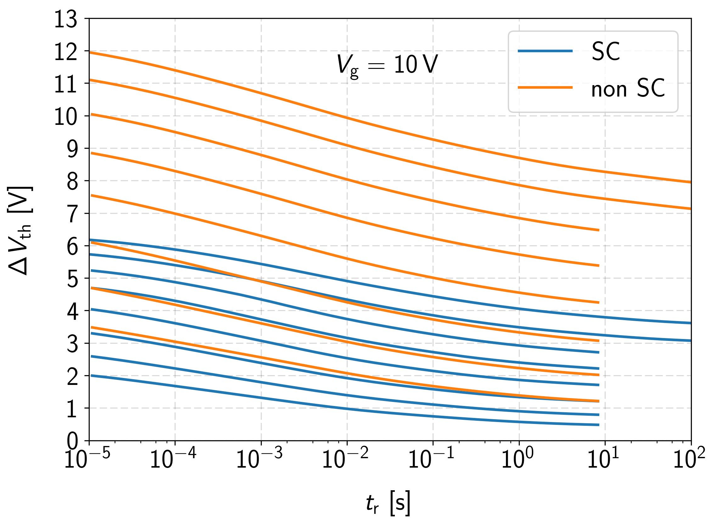
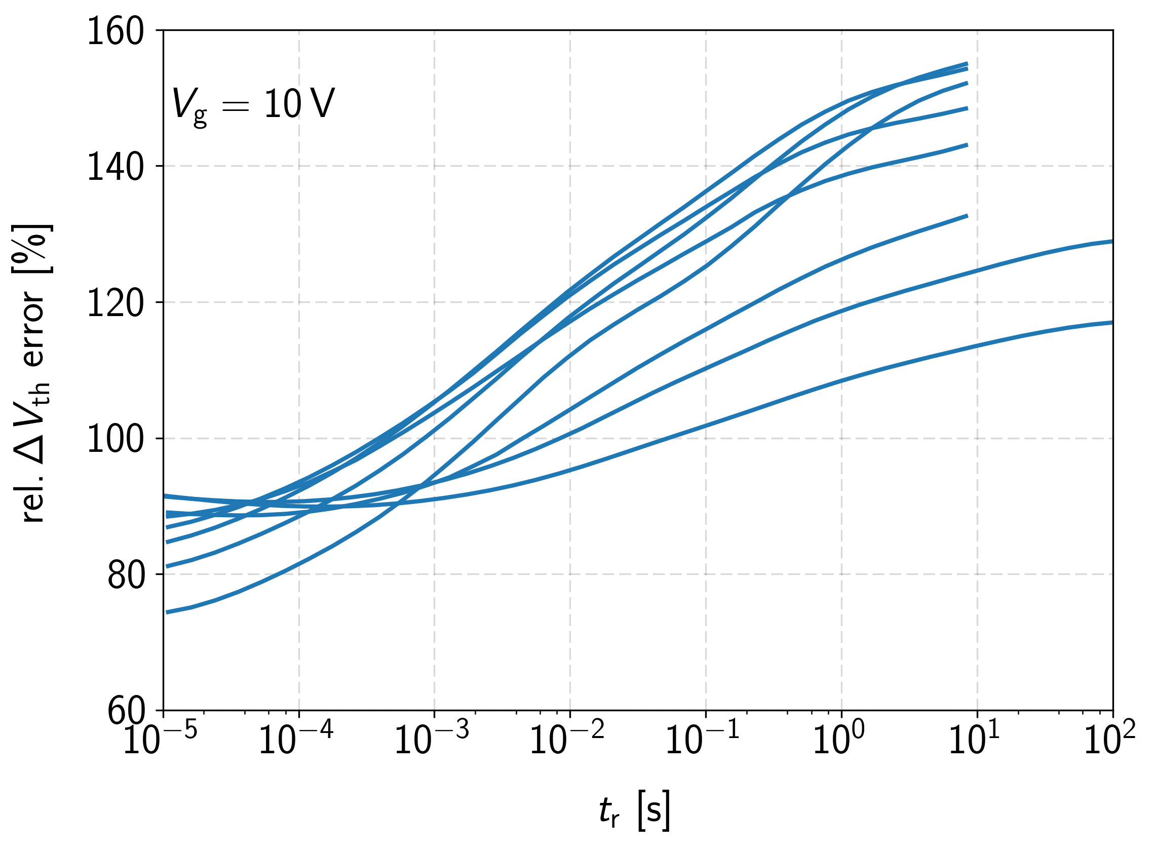
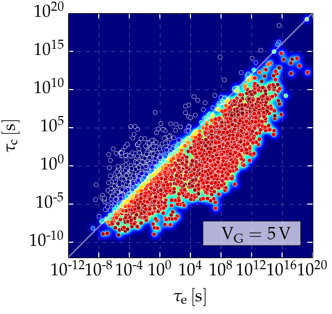
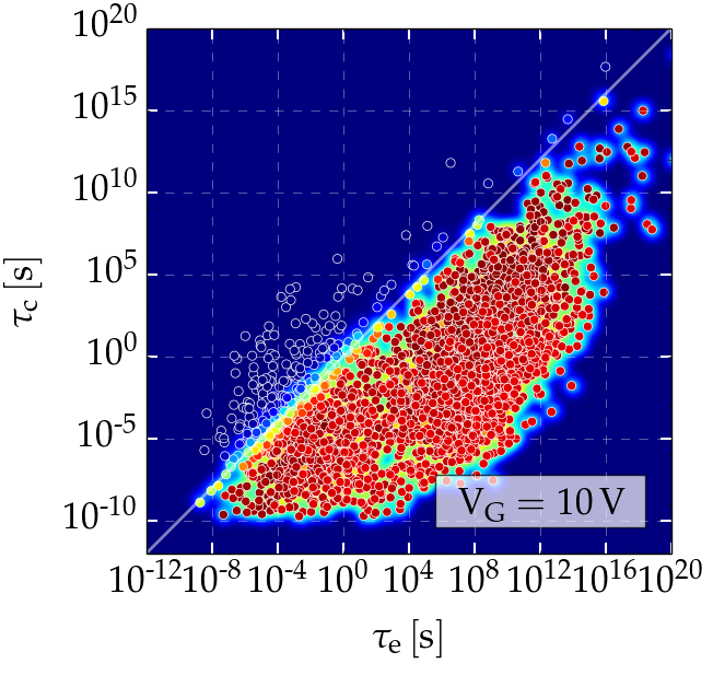
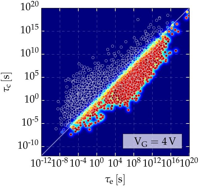
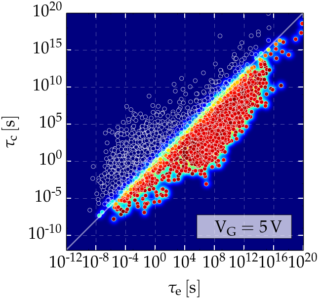
The overall impact of the charge feedback on the capture and emission dynamics of the device can be seen if the same set of defects is simulated once self-consistently and the other time non-self-consistently. As can be seen in Figure 7.6 the amount of degradation is overestimated by a factor of about 2 if the trapped charges are not considered in the simulations. Moreover, it is not just the amount of trapped charges that changes but also their kinetics. These changes in kinetics can be seen best if the relative error between the two simulations is plotted (Figure 7.7). For low recovery times the error, although still huge, is smaller compared to higher recovery times. The general trend can be explained by a simple accumulation effect of the errors made at each instant in time. For a constant relative error, the accumulated errors need to have a linear relation. Thus the nonlinearities show that also the dynamic behavior during recovery changes. Another finding in this figure is that for longer stress times, the relative error decreases (the 100 s traces are related to stress times of 1 s and 10 s). This can be explained by a charge saturation effect similar to [66].
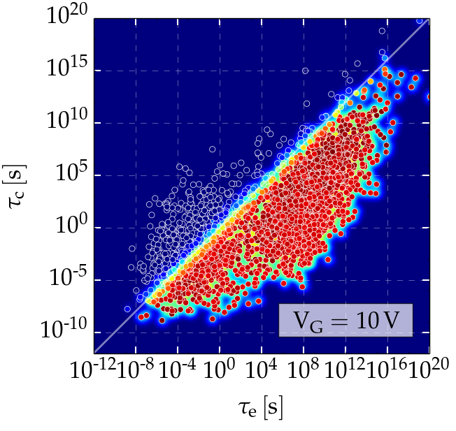
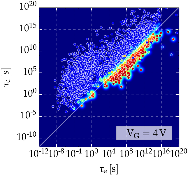
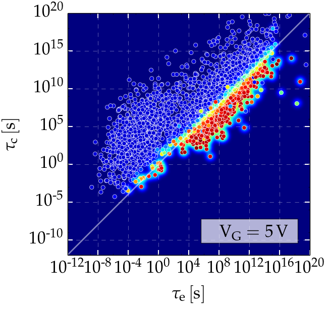
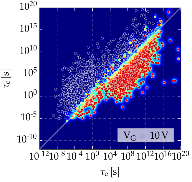
In a first-order approximation, these nonlinearities can be attributed to changes in the active energy area and the trap levels as mentioned earlier in the text. The changes due to charge feedback can be best understood when looking at the CET maps [195] of the defects at different stress bias for different instants in time, see Figure 7.8. At the beginning of the first stress cycle most of the defects, previously being empty, are brought into the active energy area where they can potentially capture an electron (top row). If a significant amount of them captures a charge, the positive charges present at the dielectric interface decrease, causing an increased surface potential. During recovery, not all charges can be emitted so subsequent stress cycles will experience an increased surface potential. This potential shift causes a higher trap level for the electrons, decreasing the amount of trapped charge as compared to a fresh device. The very same mechanism is responsible for the change in the active energy area too, where the residual surface potential shift lowers the effective oxide field during stress. Because of that, even for longer stress times only a smaller amount of defects is able to capture a charge.
The residual amount of trapped charges of course strongly depends on the applied stress voltage, the stress time and the recovery period allowed between two subsequent stress cycles. In the second row of Figure 7.8 the defects after the last stress cycle are plotted. Electrostatic charge feedback, which was explained in the last paragraph, then already caused a significant shift of the time constants towards larger values. The asymptotic limit of this mechanism can be seen in the third row, where the thermodynamic equilibrium of the defects is shown. Note that the shift of the time constants as compared to the transient results covers additional five orders of magnitude.
The changes in the trap level and the active energy area are however not the only feedback mechanisms that can potentially influence the defect kinetics. For example, local changes in the potential caused by a single charge captured by a defect can influence the capture and emission times of neighboring defects. On top of that, the spatial distribution of defects could cause an inhomogeneous lateral surface potential profile. A third mechanism would be band bending due to the vertical distribution of defects in the oxide.
Accurate modeling of those effects is troublesome, as their individual influence on the overall degradation cannot be separated well enough. While the first two effects could in principle be tackled by adjusting the spatial distribution of interface and oxide defects, the latter one is much more difficult to describe. Due to the non-local nature of the NMP defects, corrections for the local potential fluctuations across neighboring grid points would need to be calculated. Concepts like direct interactions between defects are even harder to implement as they would require to solve large systems of equations and accurately extrapolate some of the grid quantities to the place of the defect. A basic discussion about different methods to estimate the influence of a charged defect on the local potential surface can be found in Section 7.2.4.
In this section it was shown that the forward bias drift observed in large-area GaN/AlGaN MIS-HEMTs can accurately be modeled by two sets of normally distributed NMP defects. A careful selection of key parameters for the device simulation like the amount of polarization induced charges, bulk dopings and transport mechanisms in the barrier layer
allowed to thoroughly investigate different feedback mechanisms having an influence on the experimentally observed capture and emission times. The most important one was identified as the change in the surface potential due to charge trapping, resulting in increased defect levels and a decreased active energy area
seen by the defects.
Due to these effects, modeling approaches like the usage of accumulated stress times cannot be used as the observed defect kinetics are a strong function of previous stress and recovery cycles in the device. Thus, for this kind of devices, it is of utmost importance to use transient simulations following the experimental bias conditions as closely as possible.


