In BTI measurements on large-area devices, only the response of a large ensemble of defects can be identified because the electrostatic impact of a single defect cannot be resolved by the measurements. In a simple charge sheet approximation, this can be explained by the charges stored in a capacitor being directly
proportional to the capacitance at a fixed gate bias. Thus the relative impact of a single charge grows for small-area devices. The ongoing downscaling of devices allowed to identify charge transition events of single defects as step functions, first observed as RTN in the 1980s [106–108]. The link between RTN and the  noise in large-area devices was found in 1984 by Uren et al. [107].
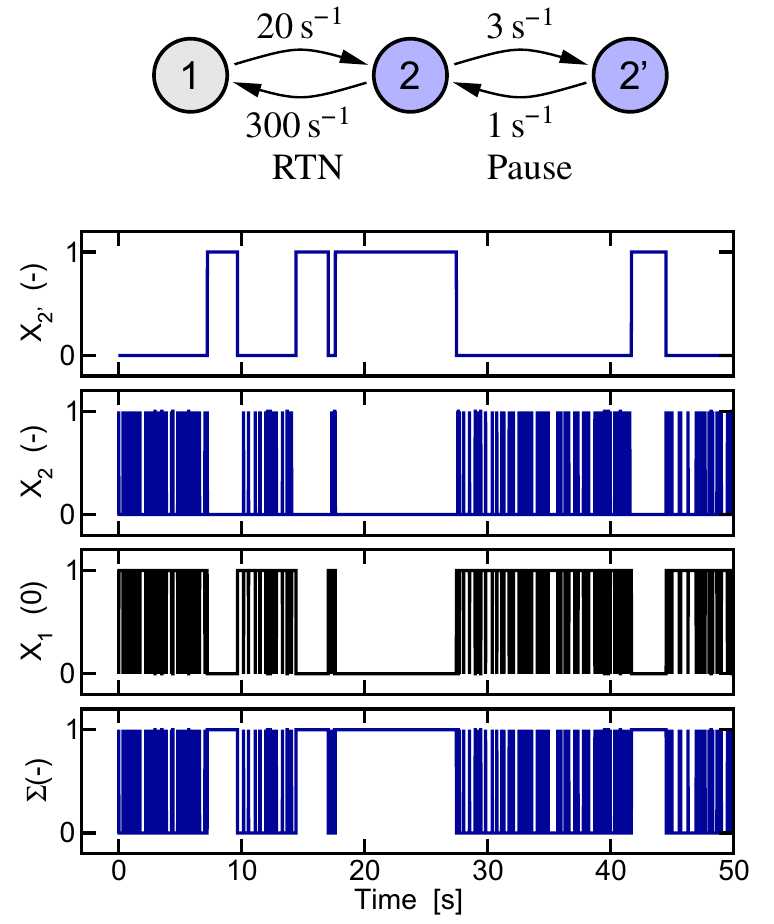
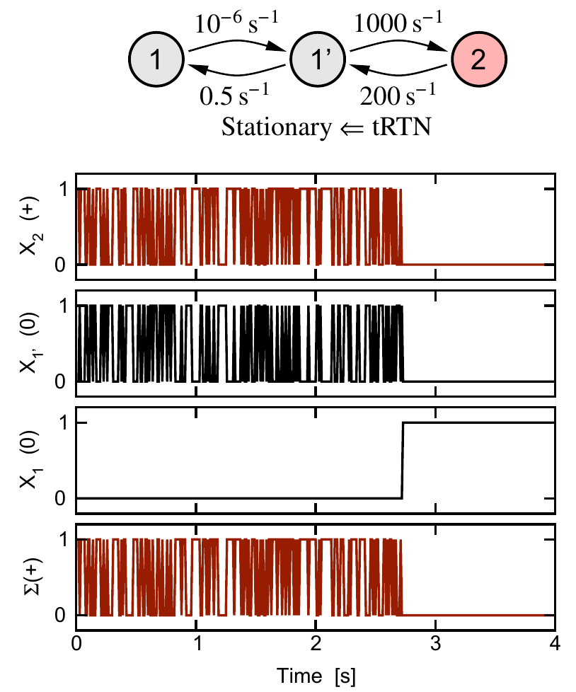
Since the first observations of single defect transitions in the 1980s, several different types of complex RTN signals have been identified and successfully linked to single defects with multiple states. The term anomalous RTN was introduced to describe regular two-level or three-level RTN interrupted by inactive phases [108]. In this work, the authors already put forward CC diagrams of three-state defects including a metastable state which later became the basis for using NMP models with metastable states to describe BTI degradation [109, 110]. A closely related phenomenon is temporary RTN, where in contrast to anomalous RTN the signal does not reappear again [110]. An example of two defect configurations producing anomalous and temporary RTN can be seen in Figure 4.3.
More recent studies have also revealed evidence for a link between SILC and RTN by measuring correlated emissions in the gate and drain currents of a device [111] and linked even more complex capture and emission patterns to four-state defects with two metastable states [112, 113].
The measurement of RTN signals is simply done by applying different biases to the gate in the linear regions of the device and by continuously recording the resulting drain current. If desired, the resulting drain current fluctuations can then be mapped to  . Additional complications arise if the same measurements are performed on GaN/AlGaN heterostructures. The first one is a technological problem as the fabrication processes for MIS-HEMTs usually do not allow to produce devices down to the required size. The presence of the barrier layer additionally
reduces the expected step-sizes of the individual defects which deteriorates the SNR of the measurements. Also, the usable voltage range is limited as long-term BTI drift on top of the RTN dramatically complicates the defect parameter extraction.
. Additional complications arise if the same measurements are performed on GaN/AlGaN heterostructures. The first one is a technological problem as the fabrication processes for MIS-HEMTs usually do not allow to produce devices down to the required size. The presence of the barrier layer additionally
reduces the expected step-sizes of the individual defects which deteriorates the SNR of the measurements. Also, the usable voltage range is limited as long-term BTI drift on top of the RTN dramatically complicates the defect parameter extraction.
For GaN technology, it is thus advisable to cool down the devices as far as possible to a) reduce long-term drift by bringing as many defects out of the measurement window as possible and b) increase the SNR by reducing the thermal noise level. This is in contrast to silicon technologies, where temperatures and voltages are usually ramped up to trigger more defect responses. For normally-on devices, the voltage range is also limited to negative voltages because of their large instability in the forward-bias range.
The TDDS was derived from the deep level transient spectroscopy, which has been extended for single defects in 1988 [114]. Single defect DLTS relies on two major assumptions, namely an exponential distribution of the emission times and different step heights for each defect. In their original study, Karawath and Schulz used a statistical analysis of the emissions observed after several stress and recovery cycles at different temperatures to extract the emission time constants of the defects and calculate their activation energies [114]. It was originally also assumed that the defects are always charged after applying a certain stress to the device, thus the influence of stress time on defects with larger time constants was neglected.
The influence on the stress time on the average defect occupancies was finally accounted for with the introduction of the TDDS [115, 116]. It takes advantage of
the fact that the average occupancy  of a defect at a certain stress bias and temperature is a function of the applied stress time
  [110]:
The symbols  and
and  are the equilibrium probabilities of the defect being charged at the stress and recovery bias respectively. In TDDS measurements this relation can be used to calculate the capture time of the defect by performing a series of eMSM measurements with different stress times and count the number of emission
events of a certain defect. Given a series of
are the equilibrium probabilities of the defect being charged at the stress and recovery bias respectively. In TDDS measurements this relation can be used to calculate the capture time of the defect by performing a series of eMSM measurements with different stress times and count the number of emission
events of a certain defect. Given a series of  measurements with
  emission events of a defect at a certain stress time, an estimator of the average occupancy is given by
The confidence limits of the average occupancy above highly depend on the values of and [117]. The emission time constant can easily be calculated by taking the mean value of all emission times of a specific defect after the recovery voltage has been applied. The defects are usually visualized by two-dimensuonal
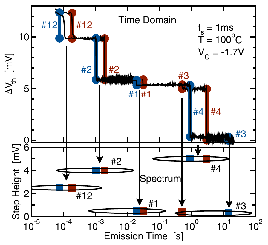
histograms called spectral maps, which contain the step-heights and the emission times extracted from the series of recovery traces for a certain stress time, temperature, and bias condition (see Figure 4.4). The observed
changes in the spectral maps then can be leveraged to extract a variety of parameters by assuming a a certain defect model (usually NMP transitions, see Section 5.2).
When compared to RTN measurements, TDDS in general can be used to characterize a larger number of defects simultaneously. In addition, they can be used to extract the time constants for a much broader voltage range because the capture time constants are derived indirectly from the emission events. This is particularly useful because it allows the sampling rate to be lower than in RTN measurements. A further optimization of the measurement window can be done by using logarithmic sampling which allows obtaining a larger maximum recovery time for a given memory depth of the data acquisition equipment.


