The ability to create normally-off devices within the GaN/AlGaN material system is essential especially for power switching applications. In addition to the previously discussed methods to create normally-off devices, like p-doped structures or recess etched devices (see Section 2.3.3), another promising approach was presented by using nano-sized fin-MIS-HEMT structures [196].
In this section, single defect parameters like the trap level and the vertical defect positions are extracted from RTN measurements on these devices at different cryostatic temperatures using spectral maps as introduced in Section 6.6.3. The question if the observed signals emerge from two coupled pairs of two-state defects or a single, more complex defect structure will be answered by evaluating the necessary coupling factors from RTN simulations and comparing them to those calculated for a chosen defect candidate using different methods. Based on these findings, two possible defect structures are investigated by extracting their characteristic time constants using HMM training.
Single-defect studies were previously used to identify defect candidates responsible for BTI in silicon devices. While defects like the oxygen vacancy could be ruled out by comparing first-principle simulations to the extracted properties, other ones like the hydrogen bridge or the hydroxyle  center are still considered to be promising candidates [86, 110, 128]. Following
the same strategy for GaN technology could help to mitigate the influence of the surface donors on BTI by engineering their electrical properties within the growth process. First attempts to passivate the interface already have been made by using forming gas anneals before the SiN deposition [197, 198] or by using Fluorine treatments [65, 199, 200]. These, however, brought only limited improvements regarding the reliability of the devices.
center are still considered to be promising candidates [86, 110, 128]. Following
the same strategy for GaN technology could help to mitigate the influence of the surface donors on BTI by engineering their electrical properties within the growth process. First attempts to passivate the interface already have been made by using forming gas anneals before the SiN deposition [197, 198] or by using Fluorine treatments [65, 199, 200]. These, however, brought only limited improvements regarding the reliability of the devices.
For regular high-power devices, the relatively high defect densities together with the inevitable feedback mechanisms as discussed in Section 7.1 make the experimental characterization of the responsible defects extremely challenging [AGC1][6, 44, 75]. Up to date, the main efforts to relate different reliability issues like current collapse, on-state resistance degradation or voltage breakdown to charge trapping were focused on bulk-type defects (see Section 3.2.1 and [55]). While this strategy seems reasonable for current degradation phenomena and drain voltage breakdown, other reliability issues like BTI and gate voltage breakdown cannot be understood correctly without taking into account the defects within the insulator as well as those at the barrier/insulator interface.
The latter have been shown to be dominant especially at forward gate bias conditions [44, 65, 75] when the polarization field in the barrier is compensated by the gate bias (overspill region). The fact that large area devices contain ensembles with a very large number of defects at the interface with broad distributions of capture and emission times further complicate the analysis of individual trap properties [AGC1][75]. To gain a better insight into the physical mechanisms of charge trapping and possibly the nature of the involved defects, nanoscale devices are very promising because they allow investigating individual single-defect properties.
In silicon technology, fin FETs have been widely adopted in state of the art technologies due to their improved gate coupling, allowing chip designs with lower gate delays and increased energy efficiency as compared to planar technologies [201–203]. However, the operation principle of the devices investigated in this thesis is entirely different from those in silicon technology due to the native electron channel present at the GaN/AlGaN interface. Figure 7.9 shows schematic pictures of a regular silicon fin FET and the GaN/AlGaN fin MIS-HEMTs used in this work. For the silicon device, the inversion channel is concentrated at the oxide interface, while for the GaN device the channel is located at the channel/barrier interface.
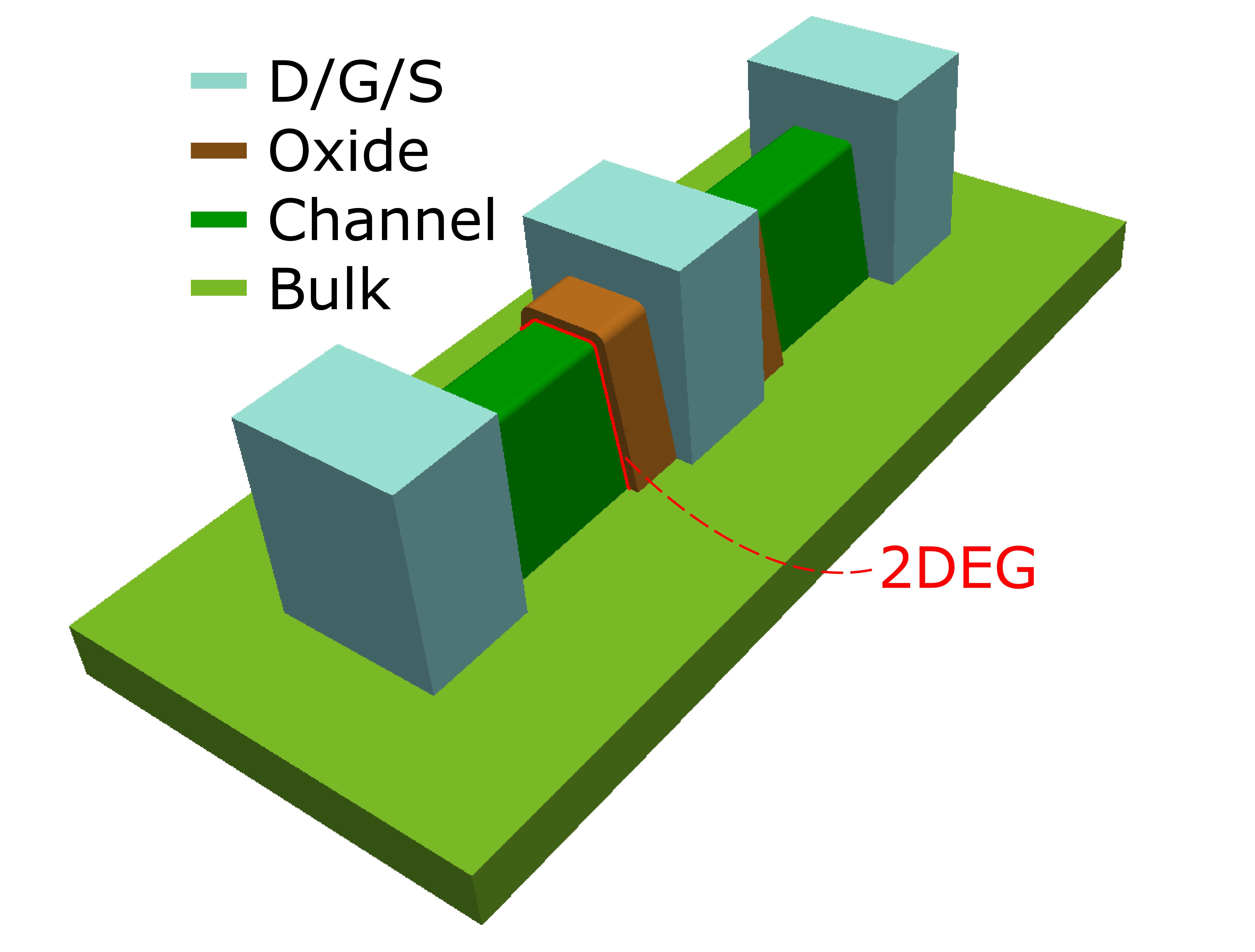
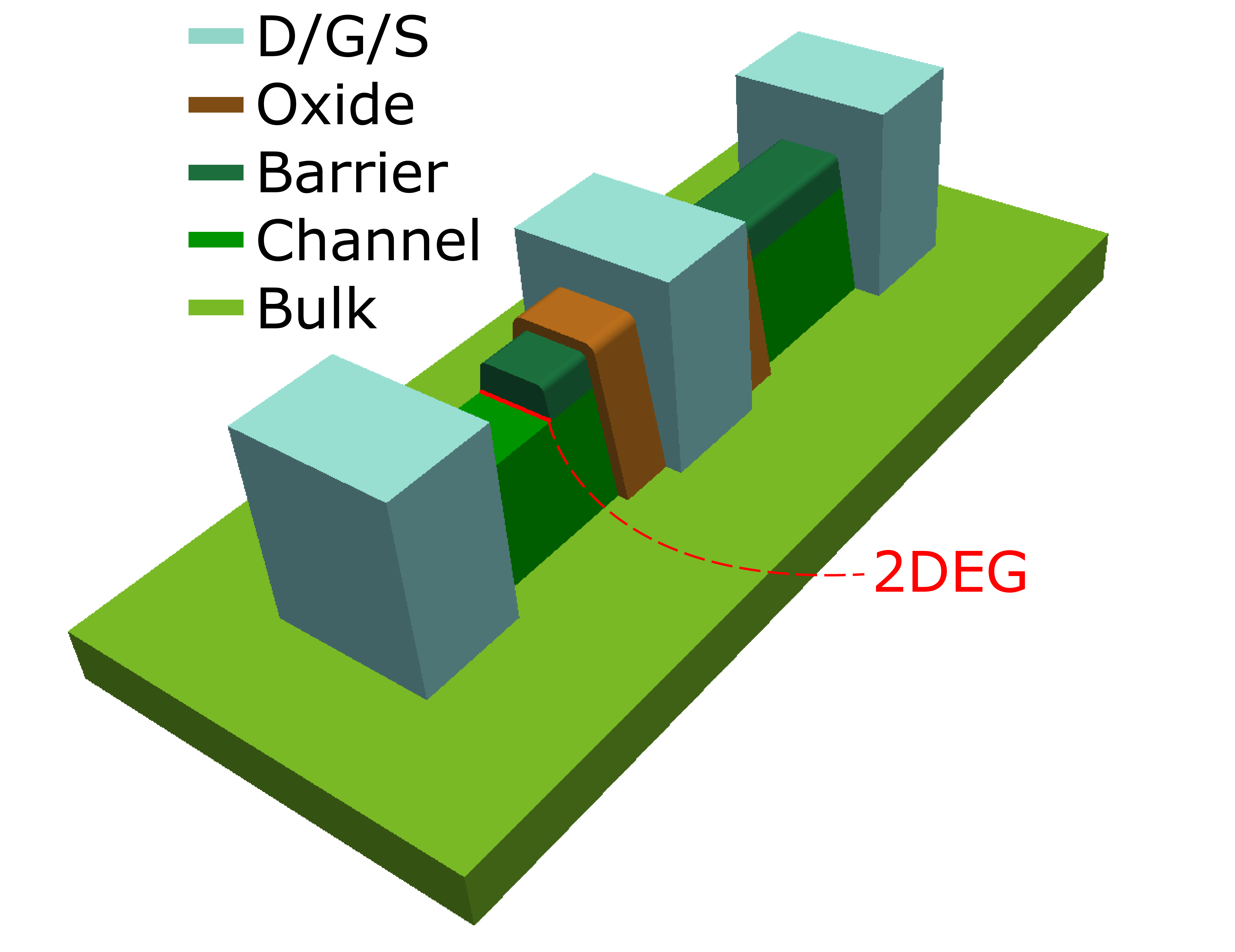
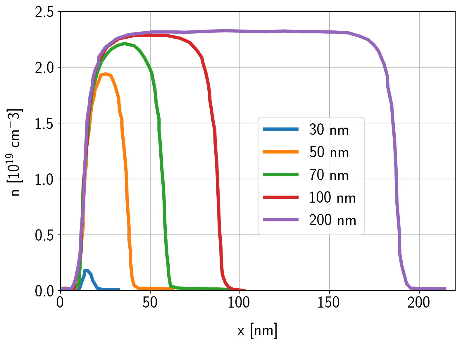
This peculiarity has some interesting consequences. First and foremost it enables to geometrically engineer the sheet carrier density independently from the aluminum content of the barrier as shown in [196, 204]. The mechanisms behind that are thought to be the depletion of the channel from the sidewalls as well as a partial relaxation of the strain induced polarization charges. A simulation study in [204] showed horizontal cuts through the channel for different fin widths. As can be seen in Figure 7.10, for wider fins the sheet carrier density is dominated by the polarization charges. At about 70 nm and below, the channel is more and more depleted, leading to positive threshold voltages for narrow fins.
Unlike the devices investigated in [204] which were fabricated with Schottky gates, the devices in this work were insulated by a 20 nm thick high-quality aluminum oxide layer. The HEMT was formed by a 30 nm thick AlGaN barrier (30% Al) on top of a 80 nm GaN channel layer and a 2 µm thick highly resistive GaN buffer. The lateral dimensions of the fin were about 50 nm x 1 µm.
The fin structures were formed by electron-beam lithography and a subsequent wet-etch removing the barrier and the channel layers. Due to that, parasitic heterojunction free MOS devices are formed at the sidewalls and the highly resistive GaN bulk. A more detailed description of the devices and the fabrication can be found in [196]. The parasitic GaN MOSFETs add a second operation regime to these devices where at positive gate voltages majority carriers are accumulated and notably contribute to the overall drain current.
The two operating regimes, regular 2DEG conduction and sidewall accumulation are shown in Figure 7.11. The 3D-simulations were carried out with Minimos-NT [21] on a simplified geometry where the access regions as well as the source and drain regions were scaled in order to speed up the computations. The piezoelectric charges at the hetero-interface were chosen according to [192] and a thermionic field emission model was used to calculate the transfer of electrons and holes across the heterointerface at the channel. The doping concentrations and the compensation of the piezoelectric charges at the barrier-oxide
interface were calibrated using  characteristics at different temperatures. More precisely, the doping concentrations were obtained by utilizing the sidewall accumulation regime as shown in the right picture in Figure 7.11, which adds to the slope of the on-current in the characteristics and produces a second kink at about
  (Figure 7.12).
characteristics in these devices (see Figure 7.12 and [196, 205]).
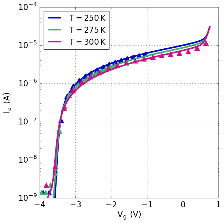
characteristics of the device at different temperatures. The accumulation regime at positive gate voltages can be seen as an additional kink in the curve at room temperature. Since the curves have been recorded prior to each RTN measurement sequence, they have been corrected by the accumulated
BTI-related  shift (from [AGC5]).
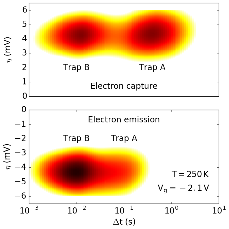
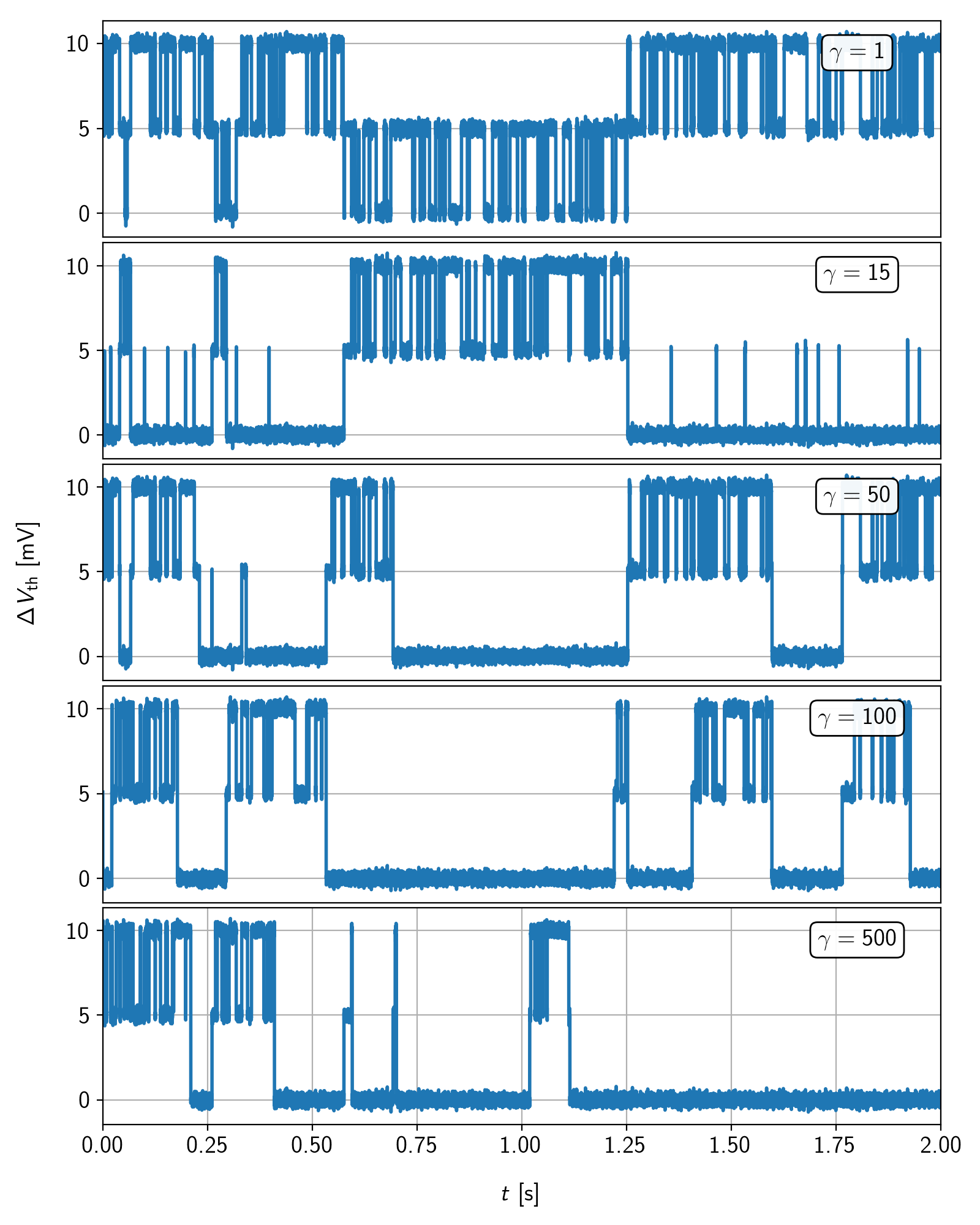
In this section, the spectral method presented in Section 6.6.3 will be used to obtain the defect properties of four dominant defects observed in a nanoscale GaN/AlGaN fin MIS-HEMT [AGC5]. Examples of the measured RTN signals of the dominant defects are given in Figure 7.13. At this point, the observed capture and emission events are treated as separately for each level, leading to four different defects called ‘A’, ‘B’, ‘C’ and ‘D’. Later it will be shown that it is rather unlikely that the observed traces were created by two pairs of coupled defects for different reasons.
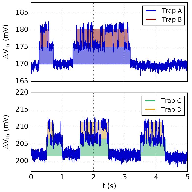

 . The emissions ‘B’ and ‘D’ are only active if in ‘A’ and ‘C’ an electron has been captured. When treated as separate defects, this fact together with the similar step heights indicates that the traps would be in immediate vicinity to each other. The sampling frequency for all measurements was 10 kHz.
For illustration purposes, the signal is shown after filtering with a median filter. Right: Two possible Markov chains resembling the observed correlated RTN signals. The similar step heights together with the correlated emissions either indicate a strong coupling between two independent two-state defects
(top) or a single three-state defect with one electron captured for each state (from [AGC5]).
. The emissions ‘B’ and ‘D’ are only active if in ‘A’ and ‘C’ an electron has been captured. When treated as separate defects, this fact together with the similar step heights indicates that the traps would be in immediate vicinity to each other. The sampling frequency for all measurements was 10 kHz.
For illustration purposes, the signal is shown after filtering with a median filter. Right: Two possible Markov chains resembling the observed correlated RTN signals. The similar step heights together with the correlated emissions either indicate a strong coupling between two independent two-state defects
(top) or a single three-state defect with one electron captured for each state (from [AGC5]).
After step detection and the extraction of the delta times for capture and emission events, spectral maps similar to Section 6.6.3 are constructed to extract the characteristic times of one or more different defects as shown in Figure 7.14. Since the measurement noise also affects the accuracy of the step height extraction, the clusters are spread in both directions. For noise-free signals, the clusters would only be spread in time due to the stochastic nature of the emissions. Note that for RTN signals the mean step heights for charge capture and emission for a specific defect have to be symmetric along the y-axis. To extract the characteristic times, the generated maps are simply binned into histograms according to their step heights. According to (6.20), the capture and emission times for simple two-state defects are exponentially distributed. If only one cluster is found for a specific step height, the histogram consists of a univariate exponential distribution and the characteristic time constant can be simply estimated from the mean value of the observed times. This is possible because the expectation value of an exponential distribution is the characteristic time constant of a two-state Markov chain (see (6.22)).
For more than one defect generating emissions with a certain step height, the mean values could be taken independently for each cluster. However, if the separation between the clusters in time is not sufficient, especially the minor distributions with less samples (i.e. the ones with the larger time constants) often cannot be extracted accurately. This case is depicted for the emission times in the spectral map shown in Figure 7.14. A more reliable approach is then to fit multivariate exponential distributions directly to the histogram. The only parameter that has to be chosen beforehand is the number of defects (i.e. the number of distributions). Note that the number of visible defects can potentially change with voltage and temperature.
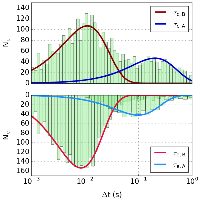
 . Right: The histograms of the capture (top) and emission (bottom) times show the number of transition events at a certain gate voltage and temperature. The capture and emission times of each individual trap can be obtained most reliably by fitting multivariate exponential distributions to the data.
Because of (6.20), the resulting parameters are equal to the characteristic capture and emission times of the defects (from [AGC5]).
. Right: The histograms of the capture (top) and emission (bottom) times show the number of transition events at a certain gate voltage and temperature. The capture and emission times of each individual trap can be obtained most reliably by fitting multivariate exponential distributions to the data.
Because of (6.20), the resulting parameters are equal to the characteristic capture and emission times of the defects (from [AGC5]).
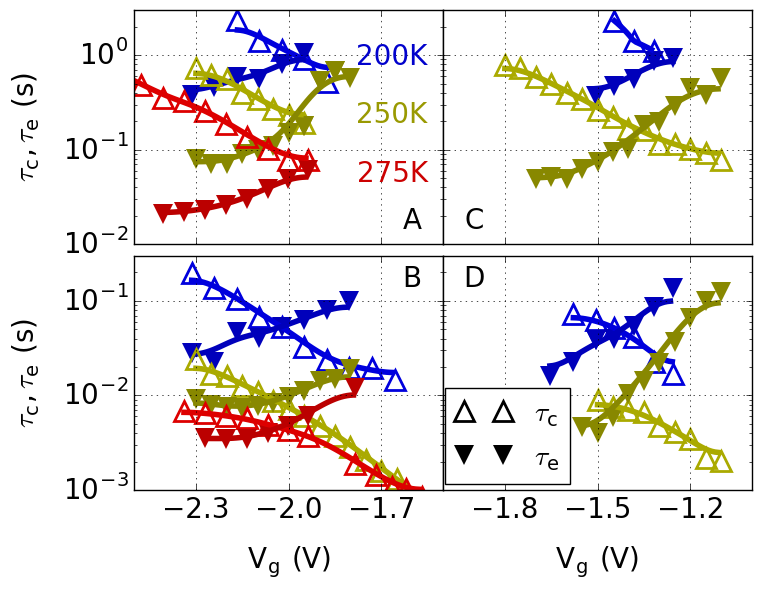
In the right picture of Figure 7.14, the resulting histogram together with the fitted distributions are shown. The mean values of the distributions correspond to the capture and emission times of the defects for a certain voltage and temperature. If this procedure is repeated for all bias conditions and temperatures, one can obtain the voltage dependence and temperature activation of all (observable) defects. The results of this extraction can be seen in Figure 7.15. Note that those characteristics were obtained without any assumptions regarding a specific physical model except the system being memoryless (i.e. being a Markov chain).
To estimate the most likely location of the traps based on the observed step heights, TCAD simulations with single charges along a horizontal cut 0.5 nm above the channel and a vertical cut through the mid-section of the device were conducted. Single electron fixed charges were placed at different positions
along the cuts and their electrostatic influence on was calculated directly from the corresponding curves. Simulations with randomly distributed dopants were conducted, leading to a distribution of step heights, compare shaded areas in Figure 7.16. The results indicate that the
defects most likely reside close to the barrier/channel interface. Deviations from the observed step heights could either be explained by the trap locations being at an especially critical place on the percolation path, double-emitting traps [206] fast enough to be sampled out from the measurement signal or some other source of variability missing in the simulations. Defect candidates for double-ionized defects have been predicted in first-principle simulations for silicon [207] and GaN technology [57]. However, the likelyhood of a double-emitting defect with the intermediate transition fast enough to be consistently missed due to sampling
can be considered low because of the related structural relaxations happening between the double-charged state and the neutral state.

curves (from [AGC5]).
More information about the defects despite their empirical voltage and temperature behavior can also be extracted directly from the curves shown in Figure 7.15 if a defect model is chosen. The bias conditions at which the RTN was observed indicate that the barrier is highly depleted, thus acting as a quasi-insulator. For that reason, band bending can be neglected and a constant field across the barrier region can be assumed. If the most simple case of a two-state NMP trap is chosen for the defect model, this enables the extraction of the trap levels, the trap positions and the activation energy of the defects observed in the measurements (see Section 5.2 and band diagram in Figure 7.17).


 was taken from the simulations conducted in Section 7.2.2.
Starting from the reaction barriers  for electron capture and
  for electron emission, their bias dependence is used to extract the aforementioned properties. The Arrhenius equation in its logarithmic form reads:
The bias dependence of the reaction barriers is given by the partial derivative with respect to  and cancels out the exponential pre-factor
  (assumed to be independent of the gate bias).
The energy difference between capture and emission barriers is equivalent to the shift of the barrier potential at the location of the trap because the ionization energy of the trap to the local conduction band edge being constant. Thus the trap level shifts together with the local barrier potential (see Figure 7.17). This can be used to relate the bias dependence of the surface potential to the bias dependence of the capture and emission barriers.
As mentioned before, the bias conditions suggest a highly depleted barrier. Thus a capacitive voltage divider can be used to calculate the potential at the trap position from the gate voltage.
The local shift of the trap level is then a function of the vertical trap position and can be calculated from (7.6) and (7.7). Solving for the trap position  yields:
At the bias conditions of the intersection point of the curves in Figure 7.15, the trap level is equal to the Fermi-level at the position of the trap (compare band diagram in Figure 7.17). This fact can be used to calculate the trap level if the effective conduction band potential of the GaN/AlGaN interface  and the surface voltage at
  ,
,  , are known. In fact, the surface voltage at any gate voltage would be sufficient, as long as the barrier is still sufficiently depleted to neglect band bending, (i.e., the capacitive voltage divider in (7.7) is justified). In this case, the surface potential and the band offset were taken from TCAD simulations. With
  being the gate voltage at the intersection point of
  and
and  , the equation to calculate the trap level
  reads:
Another thing which can be extracted from the measurements is the temperature activation of the process. When assuming equal curvatures of the parabolas from the two-state NMP process, the energy barriers for electron capture and emission can be calculated from the energy barriers for the relaxation energy  and the minimum-energy difference
  :
:
The squares in equation (7.10) can be expanded if  is assumed, which is the case in the strong electron-phonon coupling regime. The temperature activation of the process is then dominated by the relaxation energy and the apparent activation energy can be estimated by
  as can be seen in (7.11). The Arrhenius plot of the four investigated defects in Figure 7.18 shows that all of them share about the same activation energy
  .
.
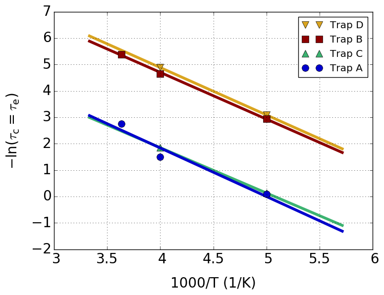
 . This observation also supports the validity of the extracted trap positions because of the crystalline AlGaN layer having a narrower distribution of defect properties than the amorphous oxide (from [AGC5]).
The summary of the extracted trap properties is shown in Table 7.1. Since the intersections of the correlated defects pairs are very similar, also the vertical positions of the traps seem to be in close
proximity to each other. For the same reason, they also share the same trap levels although the observed time constants differ by one order of magnitude. The only remaining parameters to describe the differing time constants are the exponential pre-factor  . It can be seen that the factors differ by two orders of magnitude between the slow and fast time constants, while the two defect pairs almost share the same pre-factors.
| Trap | |
 |
 |
 |
| (nm) | (eV) | (1/s) | (eV) | |
| A | 6.7 | 0.63 |  |
0.63 |
| B | 5.8 | 0.59 |  |
0.61 |
| C | 9.2 | 0.68 |  |
0.59 |
| D | 9.8 | 0.72 |  |
0.62 |
Given that the assumption of two coupled pairs of defects holds, the validity of the extracted trap parameters before primarily depends on (i) the accuracy of the step detection, (ii) the accuracy of the algorithm to extract the delta times for capture and emission times and (iii) the signal-noise ratio of the traps under investigation. The next section will investigate how to model the electrostatic coupling between two defects and how to estimate the coupling factors necessary to obtain RTN signals comparable to Figure 7.13.
In a first order approximation, the electrostatic coupling between two independent defects can be modeled as a shift of the local potential due to the Coulomb potential of a single point charge [208–211]. Other approaches calculated the change in the Coulomb energy of a given MOS system if a single defect has captured a charge [212–215].
The perturbation of the local potential caused by one defect can act on the other in two different ways, either as an additional local Coulomb barrier shifting the initial trap level or remotely via two distant traps being on the same percolation path [156, 157]. In the case of the correlated RTN observed in this work, probably the first mechanism dominates since the coupling of the time constants seems to be rather
large. This is mainly because the additional Coulomb barrier enters the equations exponentially and the supply of carriers (i.e. the percolation path) only linearly. Other arguments speaking against a lateral separation of the coupled defects are their similar step heights (i.e. trap depths) as well as the bias region they
were observed at. The coupling via percolation path would be strongest at weak channels for voltages around , however, the experiments were conducted at bias conditions quite far from that value.
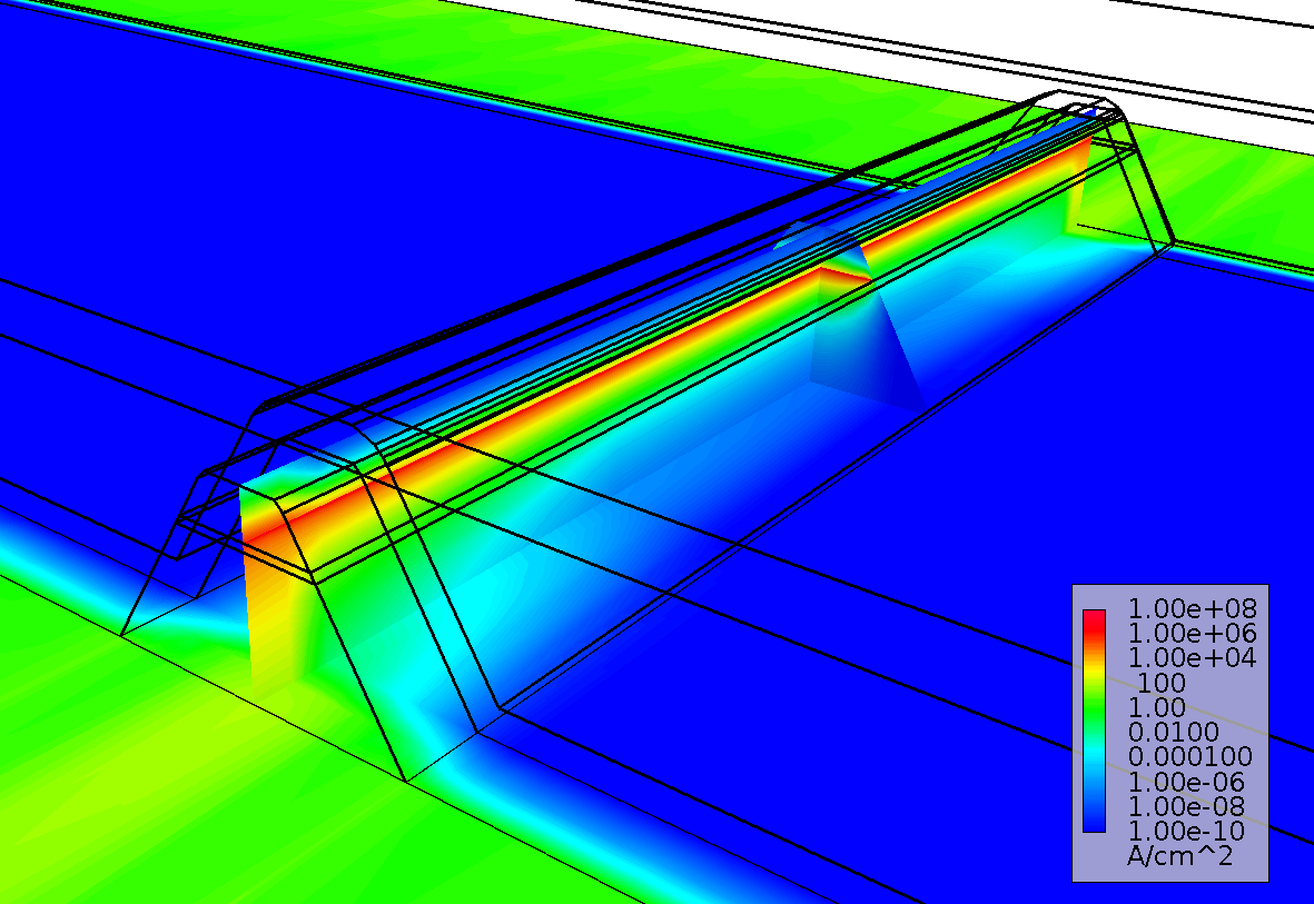
The magnitude of the potential perturbation and thus the trap level shift caused by a nearby trap is hard to predict if only classical or semi-classical simulations are available. One obvious approach is to treat defects as point charges and add them to the discretized Poisson equation. It has to be noted at this point that 3D-simulations are required for that task in order to obtain correct results. This is because the solution in two dimensions gives the potential of an infinitely long line charge. For one dimension the solution will resemble an infinitely large sheet charge, independently of discretization.
In the case of a point charge, the potential is inversely proportional to the distance to the charge. With  being the distance to the charge, the solution is given by the well-known equation for the Coulomb potential:
On the other hand, the solution for an infinitely long line charge gives a logarithmic dependence of the potential with  being the charge density and the orthogonal distance from the line:
Figure 7.19 depicts the numerical and analytical solutions for the potential of a point charge in two and three dimensions. As mentioned before, 2D-simulations cannot be used because of
the wrong overall trend (inversely proportional vs. logarithmic). In the three dimensional case and with sufficiently fine grids, the near-field impact of a single charge is overestimated whereas the far-field impact is underestimated. To overcome this problem and to be independent of grid spacing, a first order quantum
correction model like the DG model [216–218] can be used. Other approaches like the Conwell-Weisskopf model [219] divide the Coulomb potential into short-range and long-range terms, where only the long-range term enters the right-hand side of the Poisson equation. A more recent approach makes use of an analytical expression for the short-range force
acting on a particle at a distance from the charge. It resembles the Coulomb force for large distances whereas at short distances it decreases to zero, removing the singularity and rapidly changing components from the equation [220].
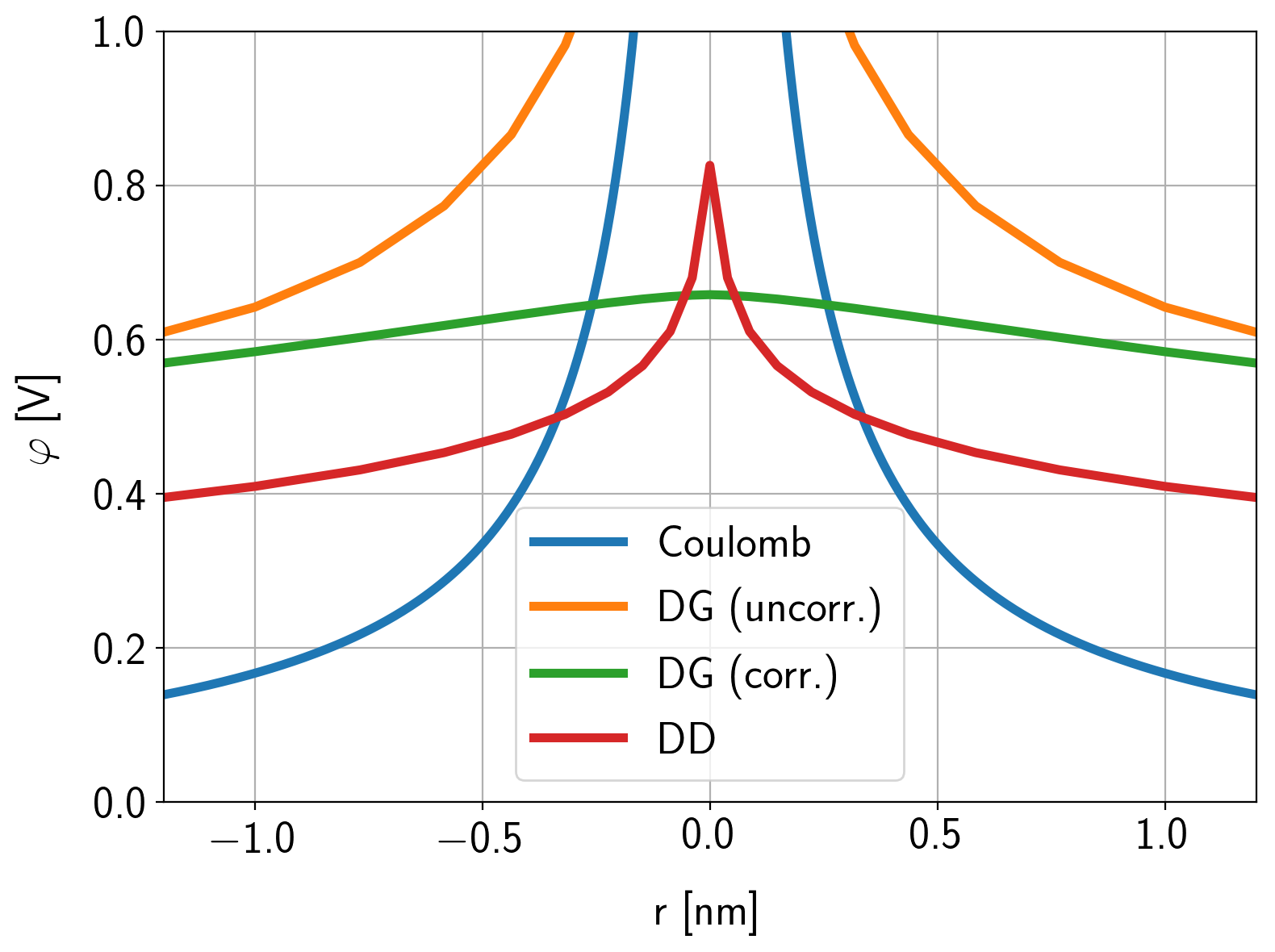
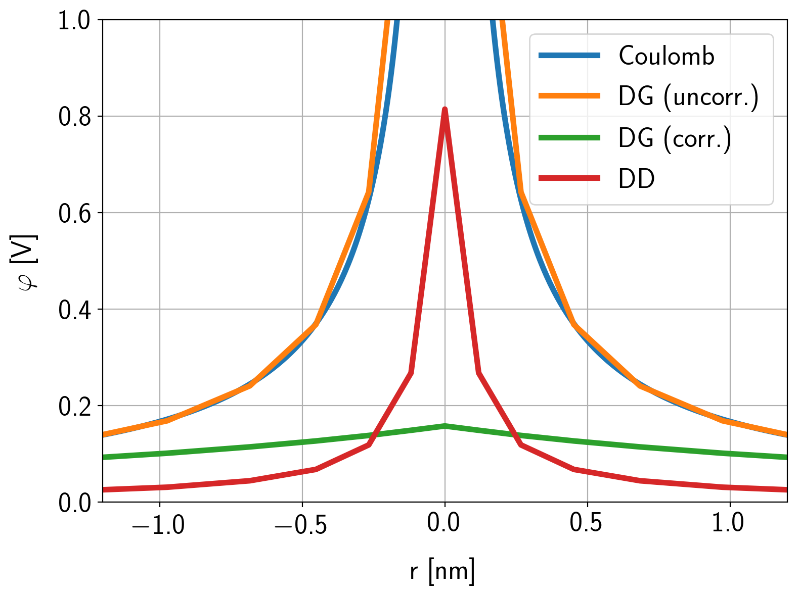
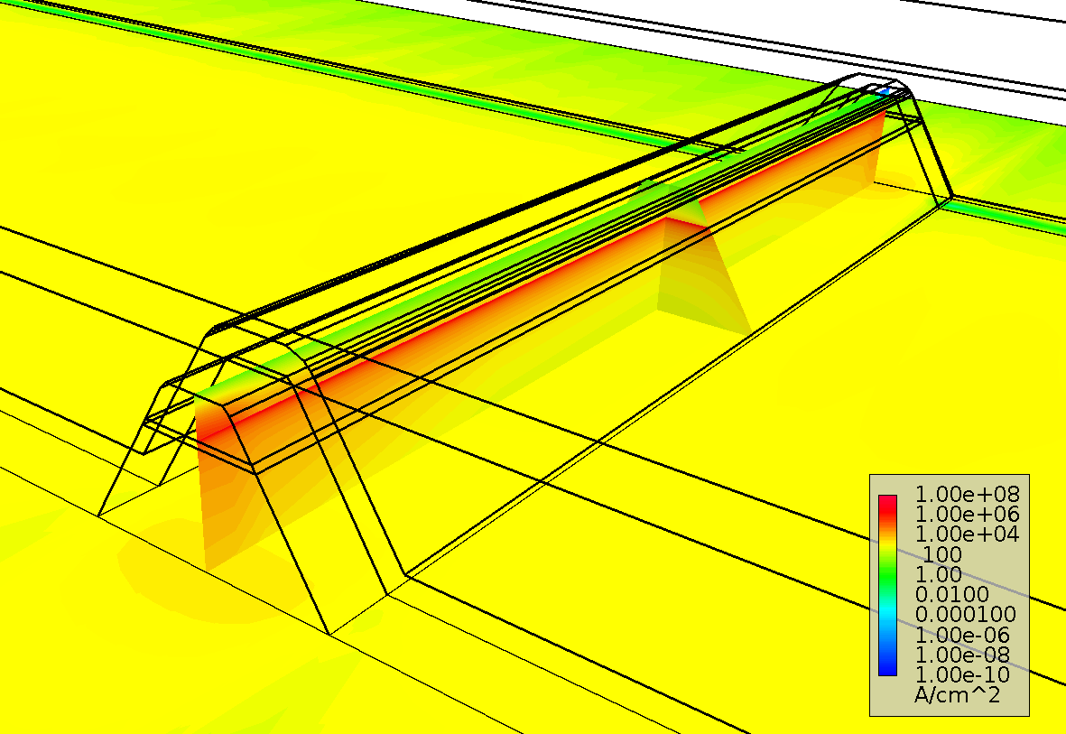
 in two and three dimensions. DD simulations are known to predict unphysical charge crowding for low grid-spacing. To overcome this problem and to be independent of grid spacing, a first order quantum correction model like the DG model can be used. Left: In two dimensions, the numerical
solution is the potential of an infinitely long line charge. This leads to an overestimation of the local impact of a single charge. Right: The three-dimensional solution correctly converges towards a Coulomb potential for intrinsic semiconductors. The density gradient model makes the local impact of a single
charge independent of the grid and only the long-range part of the Coulomb potential is considered in the Poisson equation (from [AGJ6]).
in two and three dimensions. DD simulations are known to predict unphysical charge crowding for low grid-spacing. To overcome this problem and to be independent of grid spacing, a first order quantum correction model like the DG model can be used. Left: In two dimensions, the numerical
solution is the potential of an infinitely long line charge. This leads to an overestimation of the local impact of a single charge. Right: The three-dimensional solution correctly converges towards a Coulomb potential for intrinsic semiconductors. The density gradient model makes the local impact of a single
charge independent of the grid and only the long-range part of the Coulomb potential is considered in the Poisson equation (from [AGJ6]).
This force term has its maximum at the cutoff radius  and afterwards decreases monotonically towards the point of the defect. The value of the cutoff radius should be chosen according to the physical nature of the problem. The work of Alexander [211] assumes that the maximum
of the electrical field associated with a single donor should be at the effective Bohr radius of the ground state of a donor. The effective Bohr radius for AlGaN can be calculated using the relative permittivity
and afterwards decreases monotonically towards the point of the defect. The value of the cutoff radius should be chosen according to the physical nature of the problem. The work of Alexander [211] assumes that the maximum
of the electrical field associated with a single donor should be at the effective Bohr radius of the ground state of a donor. The effective Bohr radius for AlGaN can be calculated using the relative permittivity  and the relative electron mass
  :
:
From the short-range force seen by an electron, the potential change and thus the local shift of the trap energy can easily be derived by integrating (7.14).
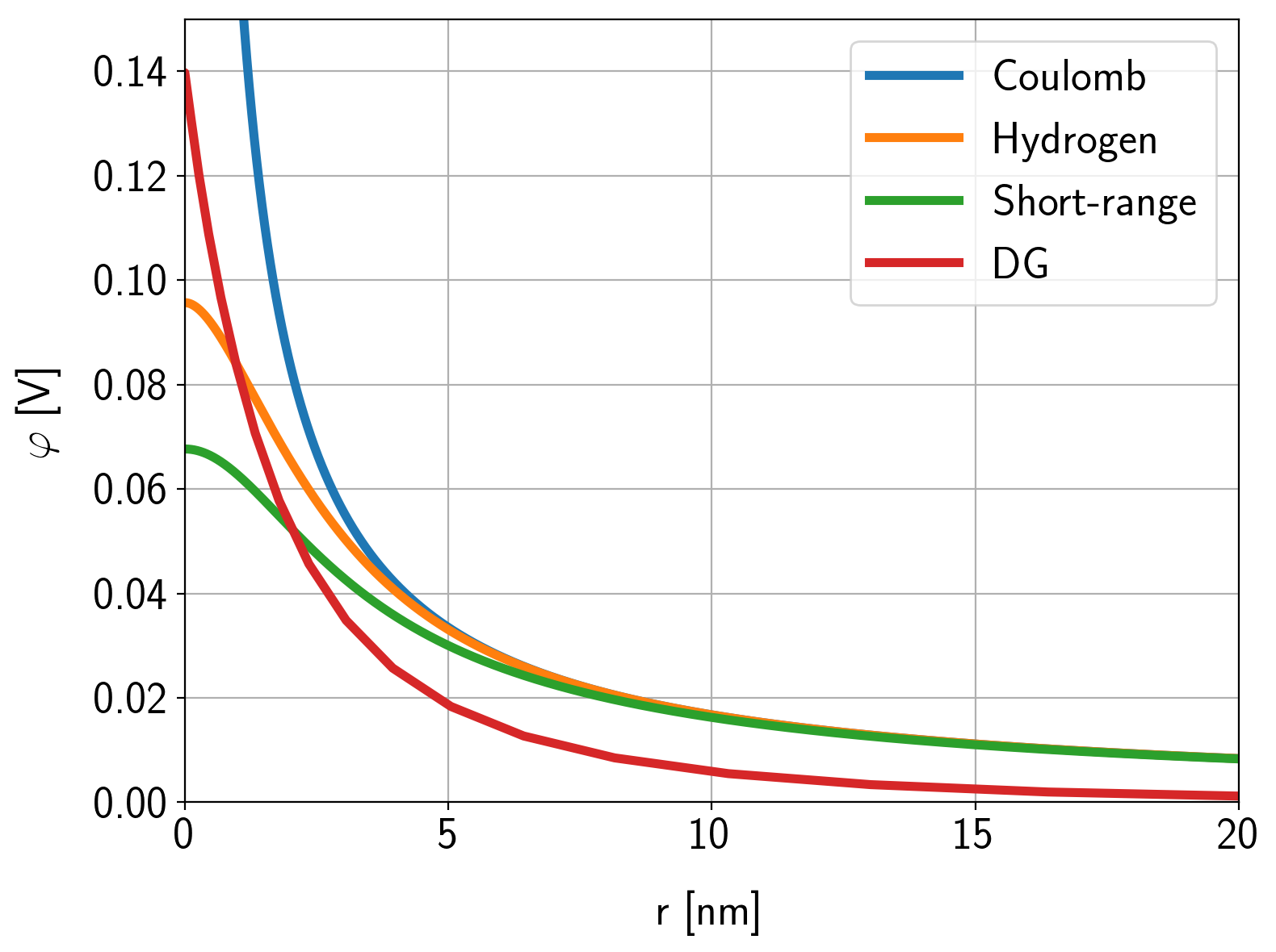
A straightforward way to check the validity of the solution provided in (7.16) is to compare it to the quantum mechanical solution for the ground state of a hydrogen atom with an effective Bohr radius as given in (7.15). The starting point of the derivation is the radial-symmetric charge density of an electron in the ground state.
By applying Gauss’ law with a spherical ansatz, the absolute value of the electric field of the electron cloud is found by:
The potential of the electron of a hydrogen atom is again calculated from the electric field by integration of (7.18).
The results of the analytic potentials versus the corrected numerical solution from Figure 7.19 can be seen in Figure 7.20. The deviation of the numerical solution from the short-range correction and the Hydrogen model could possibly be explained by two issues. The first one is due to the simulation itself, where additional screening due to the lightly doped semiconductor can influence the results. The second and probably more important one is the lack of a well-calibrated set of parameters for the density gradient model at the time of writing.
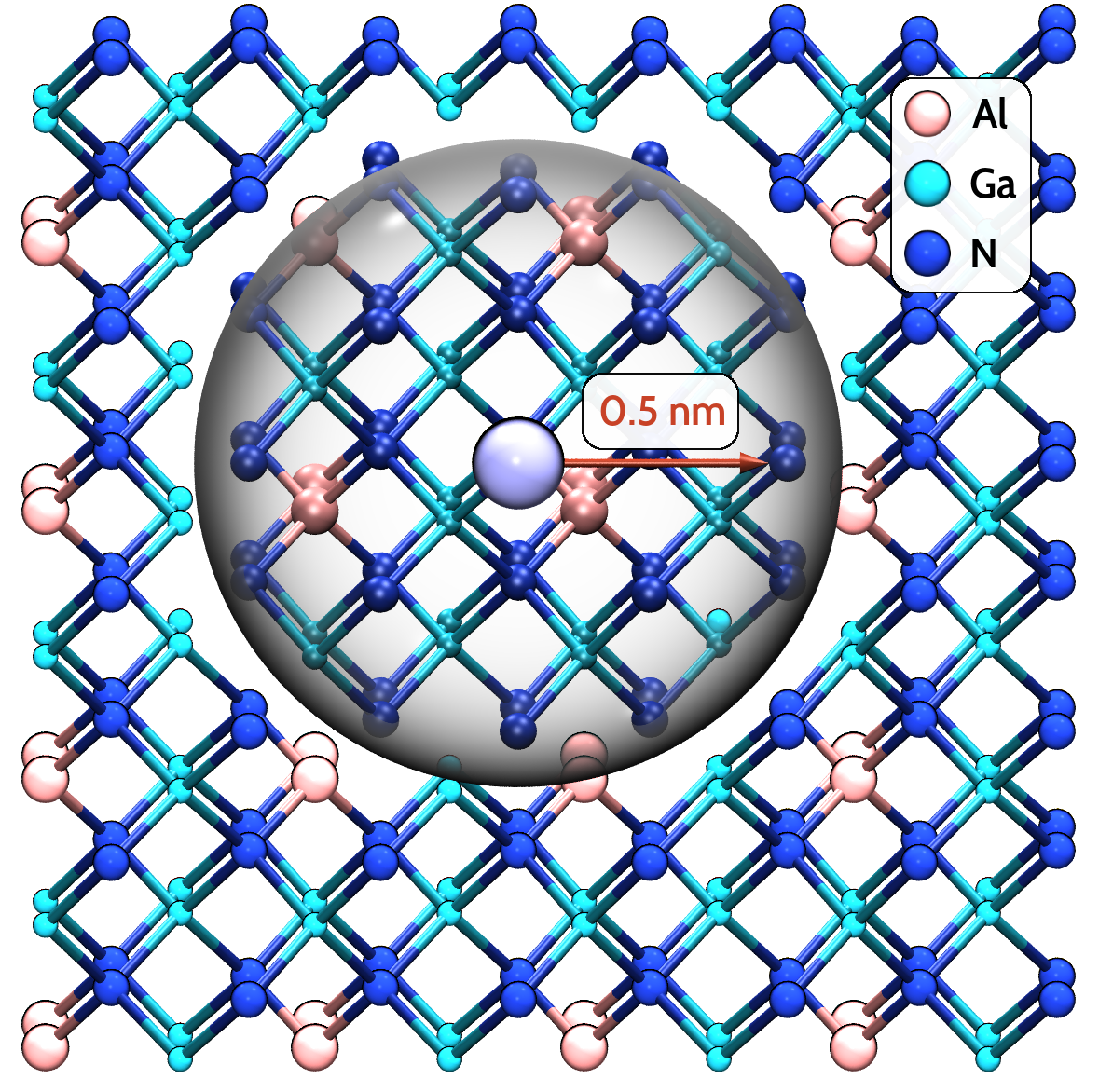
The results provided in Table 7.1 unfortunately cannot provide any information on the lateral distance between the traps, so the only way to estimate the coupling factors is to choose a suitable defect candidate based on its trap level. Due to the similar trap levels of the two coupled defects, the best guess is to make a worst-case assumption by assuming the very same type of defect in a nearest neighbor manner. Taking the values from TCAD simulations in MinimosNT, the conduction band minimum in the AlGaN barrier is at approximately 3.7 eV. Based on the data in Figure 3.1 and assuming the same absolute energy levels in the barrier as compared to GaN, the most likely candidates turn out to be either a dislocation or a nitrogen vacancy. Since the nitrogen vacancy is one of the most common defects and likely to be responsible for the n-type conduction in GaN, it is chosen for the following extraction of the coupling factors.
To calculate the minimum distance between two nearest neighbor nitrogen vacancies it has to be taken into account that the two nitrogen vacancies should not share one Ga atom. This kind of defect would distort the overall structure too much and thus is unlikely to be stable. The lattice constants of wurtzite AlGaN
alloy can theoretically be calculated based on their alloy composition  [27]:
[27]:
In the case of the investigated devices the lattice constants for  are calculated to
  and
and  . From the crystal structure in Figure 7.21, the worst-case distance between two nitrogen sites not sharing the same Ga atom was calculated to be around 5 Å, thus the
second nearest defect site has a distance of approximately 10 Å. Table 7.2 gives the resulting energy shifts for those two defects, which can easily be translated into coupling factors using
the Arrhenius law for the appropriate temperatures.
. From the crystal structure in Figure 7.21, the worst-case distance between two nitrogen sites not sharing the same Ga atom was calculated to be around 5 Å, thus the
second nearest defect site has a distance of approximately 10 Å. Table 7.2 gives the resulting energy shifts for those two defects, which can easily be translated into coupling factors using
the Arrhenius law for the appropriate temperatures.
| Model |  |
|
| 0.5 nm | 1 nm | |
| Coulomb | 335 meV | 167 meV |
| Hydrogen | 92 meV | 84 meV |
| Short-range | 66 meV | 63 meV |
| DG | 105 meV | 83 meV |
The calculated coupling factors are given in Table 7.3. If the results of the unscreened analytic Coulomb potential from (7.12) are neglected, realistic coupling factors are in the range of  to
to  . It should be noted that the provided results are a somewhat crude approximation because a structural defect in reality will always change the local configuration of atoms as well as their bonding lengths. On top of that, the hydrogen model is an oversimplification of the local potential surface which can
only be provided by first principle simulations. The results however allow quantifying a range of realistic coupling factors that could be present in a worst-case scenario. A nice first principle study on the properties of other point defects in GaN combining DFT and quantum molecular dynamics simulations can be
found in [57].
. It should be noted that the provided results are a somewhat crude approximation because a structural defect in reality will always change the local configuration of atoms as well as their bonding lengths. On top of that, the hydrogen model is an oversimplification of the local potential surface which can
only be provided by first principle simulations. The results however allow quantifying a range of realistic coupling factors that could be present in a worst-case scenario. A nice first principle study on the properties of other point defects in GaN combining DFT and quantum molecular dynamics simulations can be
found in [57].
 |
 |
|||||
| 200 K | 250 K | 275 K | 200 K | 250 K | 275 K | |
| Coulomb | 2.76 × 10⁸ | 5.67 × 10⁶ | 1.38 × 10⁶ | 16 152 | 2326 | 1150 |
| Hydrogen | 208 | 72 | 49 | 131 | 49 | 35 |
| Short-range | 46 | 21 | 16 | 39 | 19 | 14 |
| DG | 442 | 131 | 84 | 123 | 48 | 33 |
to .
Now that a range of coupling factors is known, the coupling factors required to make the vast majority of the modified RTN emissions too fast for measurements with a fixed sample rate have to be calculated. For a fixed sampling time, the mean time to emission of a defect has to be approximately one order of
magnitude below that value because of the stochastic nature of the process. In order to do that, the HMM library presented in Appendix A can be used to simulate a coupled pair of defects using the extracted time constants
from Figure 7.15 with different coupling factors. The simulation results can be seen in Figure 7.22 for a gate voltage of −1.95 V and a temperature of 250 K. To reliably suppress emissions for a sampling rate of 10 kHz as used in the measurements, a
coupling factor of about  is needed which is already at the upper limit of the calculated factors in Table 7.3. Given all the uncertainties in the derivation of the time constants and the perturbation
potentials, this result is still in range for the nearest-neighbor nitrogen vacancy. There is little literature on single defect studies focused on the coupling of traps in terms of their time constants [156, 221, 222]. These studies suggest that for strongly coupled defects, coupling factors between 10 and 20 seem to be realistic. Unfortunately they do not provide the
temperature used during their measurements. Quite interestingly, the calculated coupling factors for 300 K and 1 nm are also in the range from
is needed which is already at the upper limit of the calculated factors in Table 7.3. Given all the uncertainties in the derivation of the time constants and the perturbation
potentials, this result is still in range for the nearest-neighbor nitrogen vacancy. There is little literature on single defect studies focused on the coupling of traps in terms of their time constants [156, 221, 222]. These studies suggest that for strongly coupled defects, coupling factors between 10 and 20 seem to be realistic. Unfortunately they do not provide the
temperature used during their measurements. Quite interestingly, the calculated coupling factors for 300 K and 1 nm are also in the range from  to
to  for the last three models in Table 7.3, closely matching their observations.
is needed in order to reliably sample the modified RTN signal out of the signal (from [AGJ6]).
As already briefly mentioned in Section 6.6.3, the spectral method (together with all the other methods discussed in 6.6) share the shortcoming that the real structure of a defect is obfuscated if the defect contains thermal transitions without charge transfer. In a best-case scenario, the time constants of the inactive state are much larger than the ones of the active states and are of the same order as the measurement time for one trace. Then the spectral method completely misses that state and the emission times for the fast state are not affected at all. On the other hand, if the slow state captures and emits within the measurement window, it is going to be added as an emission of the fast state. This potentially results in a severe overestimation of the emission times of certain defects containing thermal transitions.
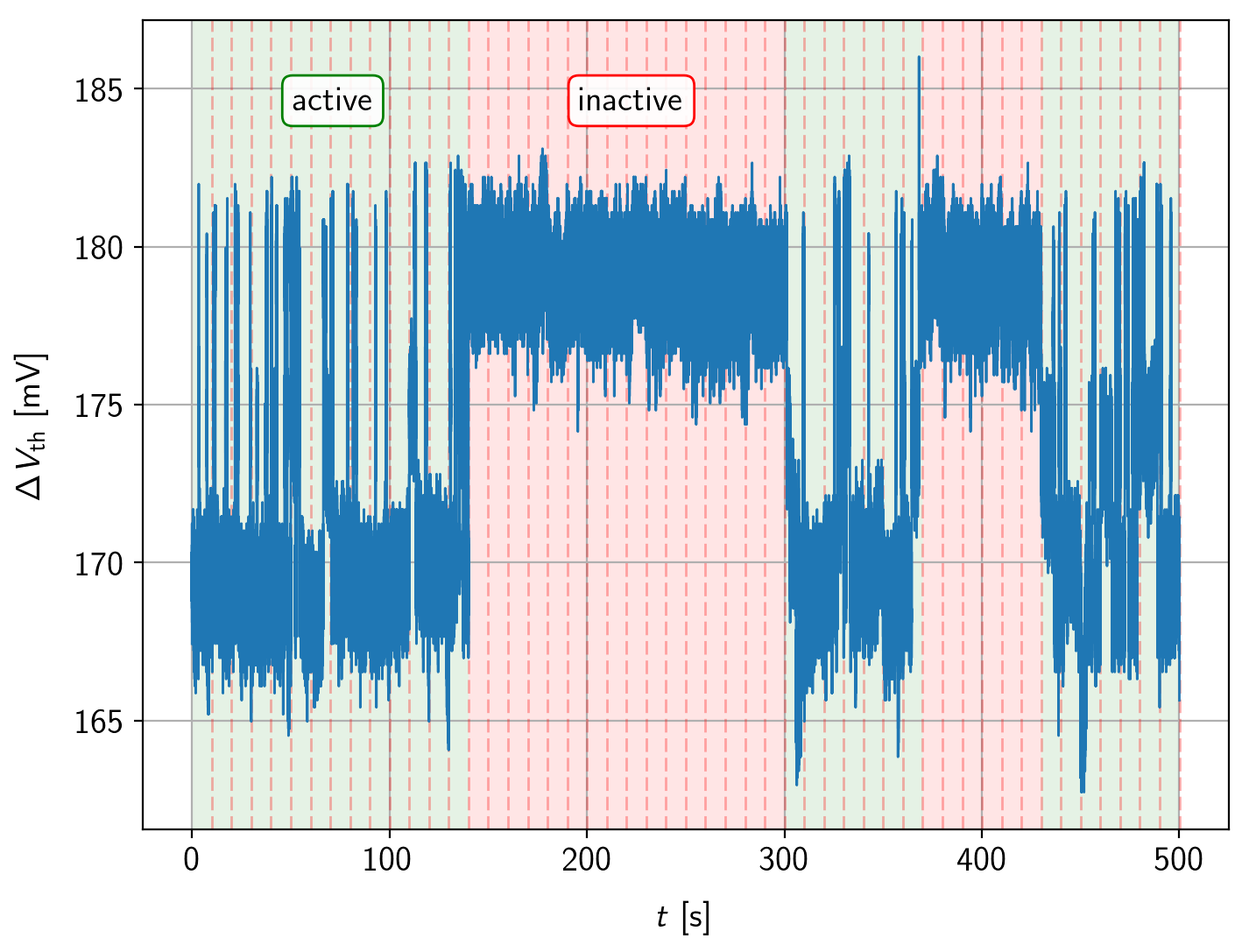
Figure 7.23 shows the measurement data from 50 subsequent RTN measurements used to extract the time constants of traps ‘A’ and ‘B’ in Section 7.2.2, merged together into one trace. It can be seen that the RTN signal becomes inactive from time to time, which is usually referred to as anomalous RTN [108, 112, 113].
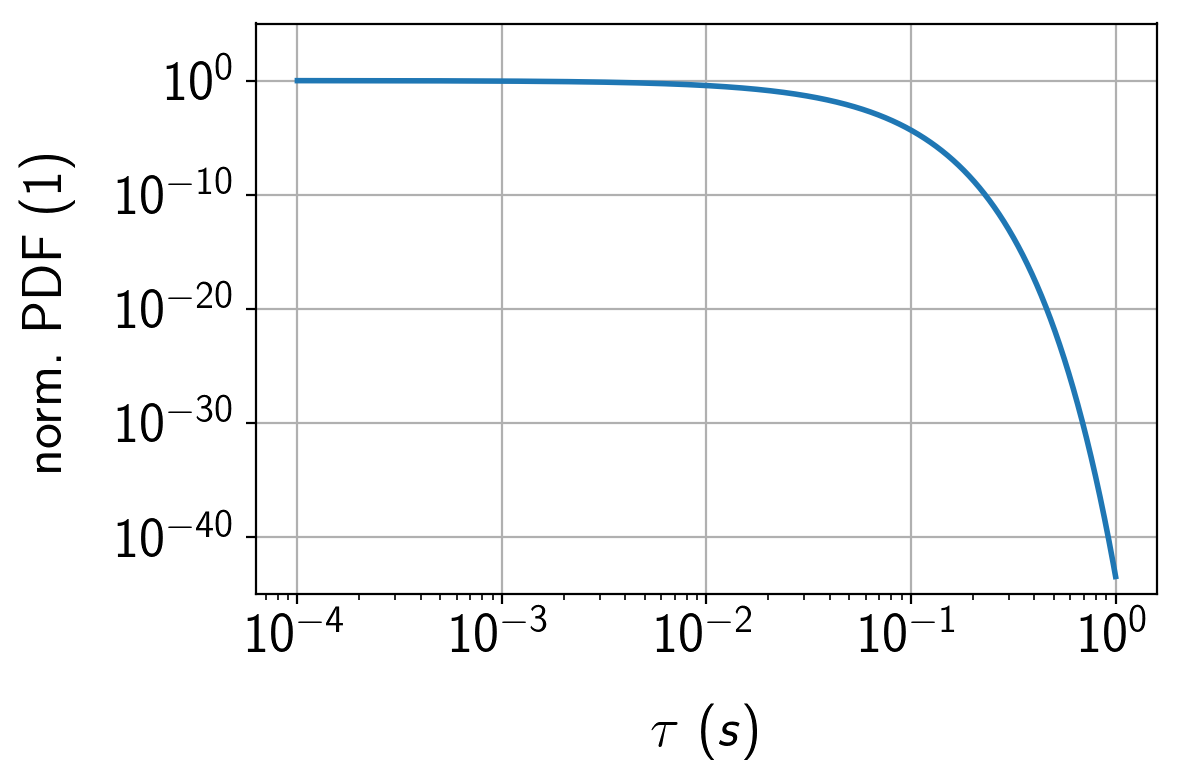
Naturally the question arises, on how to judge if a very slow emission event is just an unlucky sample of the fast state or rather should be considered as a separate thermal state. For this, the PDF of the exponential distribution given in (7.23) can be evaluated.
Figure 7.24 shows that for a trap with a mean emission time of 10 ms, the probability to observe 1 s emissions is  , which is already practically zero. Note that in the recorded RTN traces, the observed inactive times are at least three orders of magnitude larger than the extracted emission time constants of the fast trap.
tabular
 . The table on the left gives the probabilities to observe emissions being a factor
  or
or  larger. With a probability of about one in
  , a
, a  emission could still be seen as a (very) unlucky sample of the same distribution, an emission of
  from the same distribution is already practically impossible to happen in reality.
Another issue that can be seen in Figure 7.23 is that the inactive state always follows the captured state of trap ‘B’. This has serious consequences on the hypothesis of having two independent but electrostatically coupled defects. If this were the case, defect ‘A’ would have to emit its charge again during the inactivity of defect ‘B’ which should be seen in the measurement signal as a transition to the level of defect ‘A’. However, this is obviously not the case as the RTN signal stays inactive for more than 100 s at the highest level. This effectively rules out the case of two independent two-state defects, independently of the required coupling factors.
In the next step, the capture and emission times of the inactive state have to be determined. In order to be able to train the HMM, the Markov chain of the defect needs to be determined. Since the hypothesis of two coupled two-state traps was ruled out by the observation of an inactive state, it is much more likely that the observed signal is produced by a more complex defect.
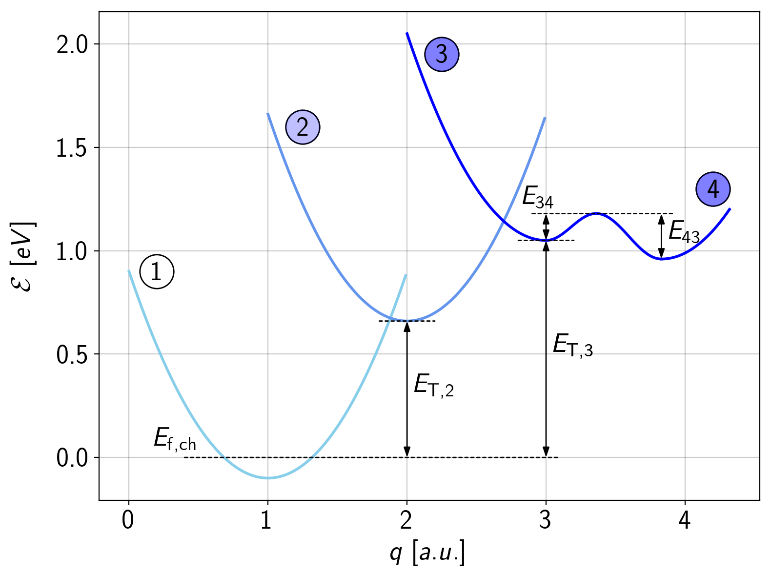
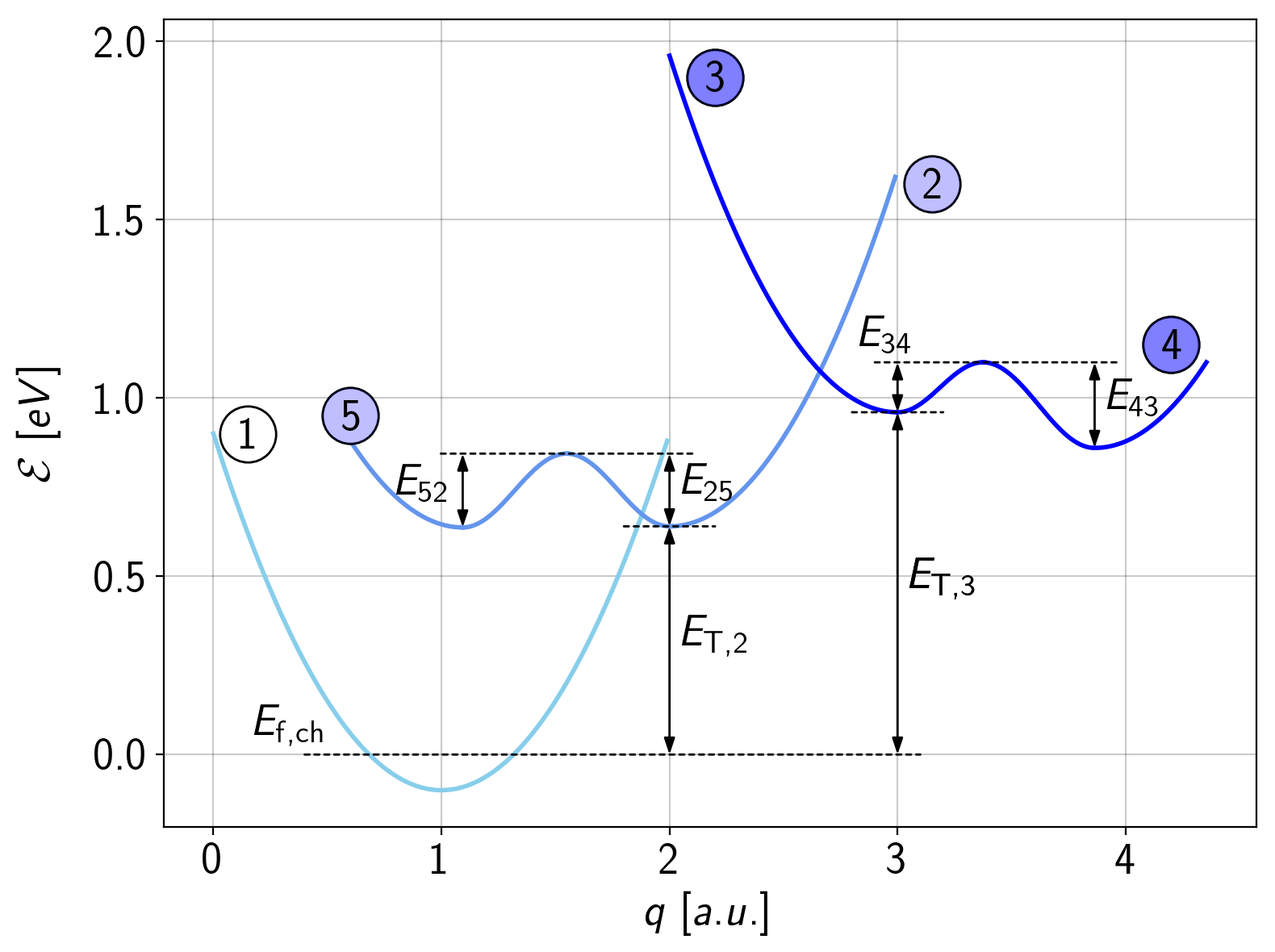
First of all, the similar step heights strongly suggest that the defect is actually capable of capturing two electrons. Because the initial charge of the defect cannot be detected, the emitting states will be plotted as neutral in its ground state  , negative in its slow state
  and double-negative in its highest state
  without any loss of generality. Secondly, since the inactive state always appears from the highest, double-negatively charged state, the thermal state is added as state
  , coming from state .
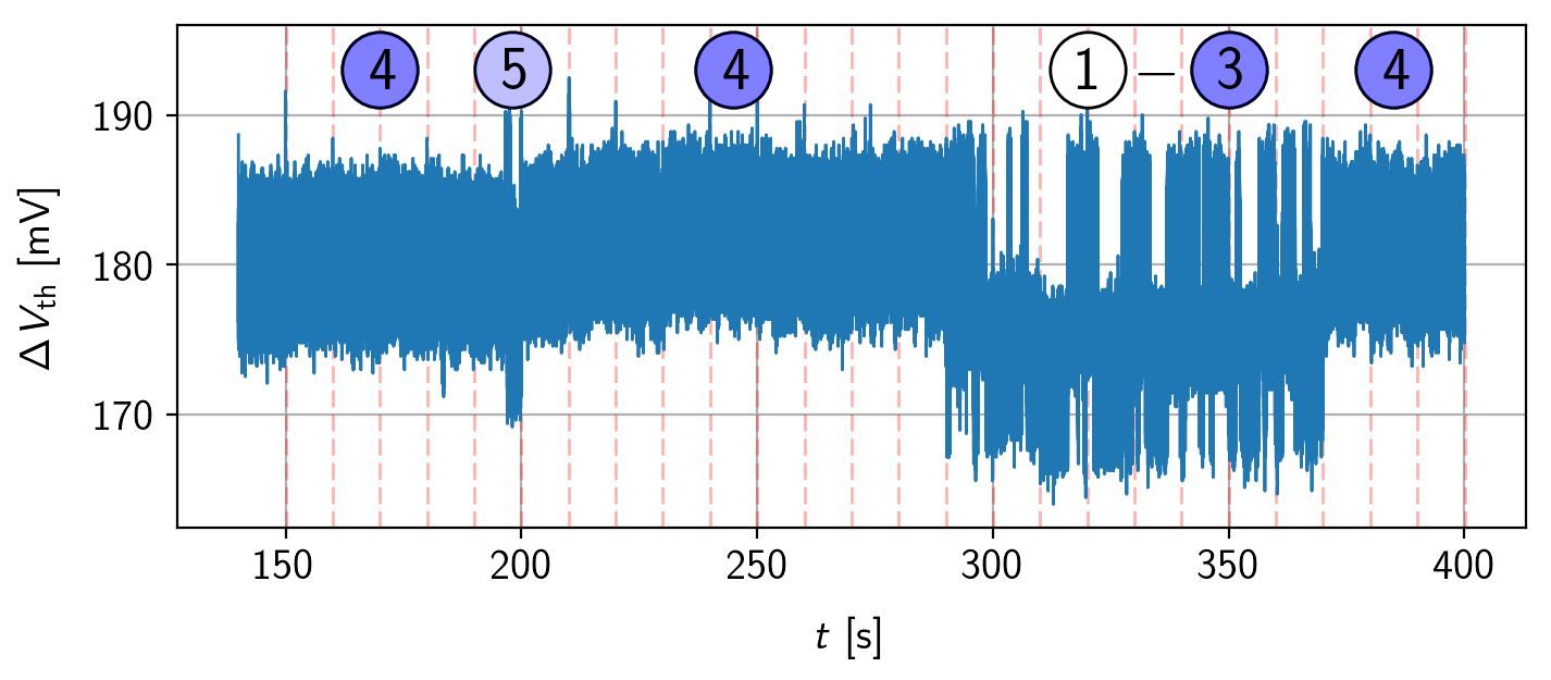
An exemplary picture of merged RTN traces useful for the selection of the Markov chain is shown in Figure 7.25. The “regular” operating regime already covered in
Section 7.2.3 is labeled with  , the inactive thermal state with . Another interesting finding is marked with
  , eventually representing another thermal state. There, after emitting an electron from state , another region of inactivity shows up. This state is seen explicitly only on a few occasions. This can possibly be explained by a significantly larger transition time from state to state as compared to the emission times from state to the other two connected states.
On the other hand, the observed time constants are approximately larger by only one order of magnitude compared to the emission times of trap ‘A’ extracted in Figure 7.15, which still is in range of a very unlucky sample of the regular distribution (compare Figure 7.24).
The two most likely Markov chains are presented in the bottom part of Figure 7.25. The thermal state(s) are added to the HMM as tied states, meaning that they possess the same
charge state (i.e. no observable emissions). In the sense of the atomic defect structure, those states most likely resemble the same kind of structural relaxation as observed in the NMP four-state model from states  to , see Section 5.2.2.


and produce the correlated RTN shown in Figure 7.13. State is a thermal state causing the inactive phases from state . Another thermal state was added because of inactivties from the fast emissions for about 5 s observed at the same level as state .
On this occasion it should be stressed that a proper selection of the Markov chains is one of the most important tasks because HMM training does not include any physical reasoning. In other words, the HMM will always stick to the pre-selected defect structure no matter how unlikely a sequence of observations will be. Sometimes the MAP probability is used to determine the number of (two-state) defects [223]. This is however a problematic approach since more defects (i.e. more levels) tend to match the long-term drift and measurement noise better and thus will have a larger probability. The best solution to this problem is to compare the temperature and bias dependence of the individual defects or defect states and judge if the Markov training delivers physically reasonable results.
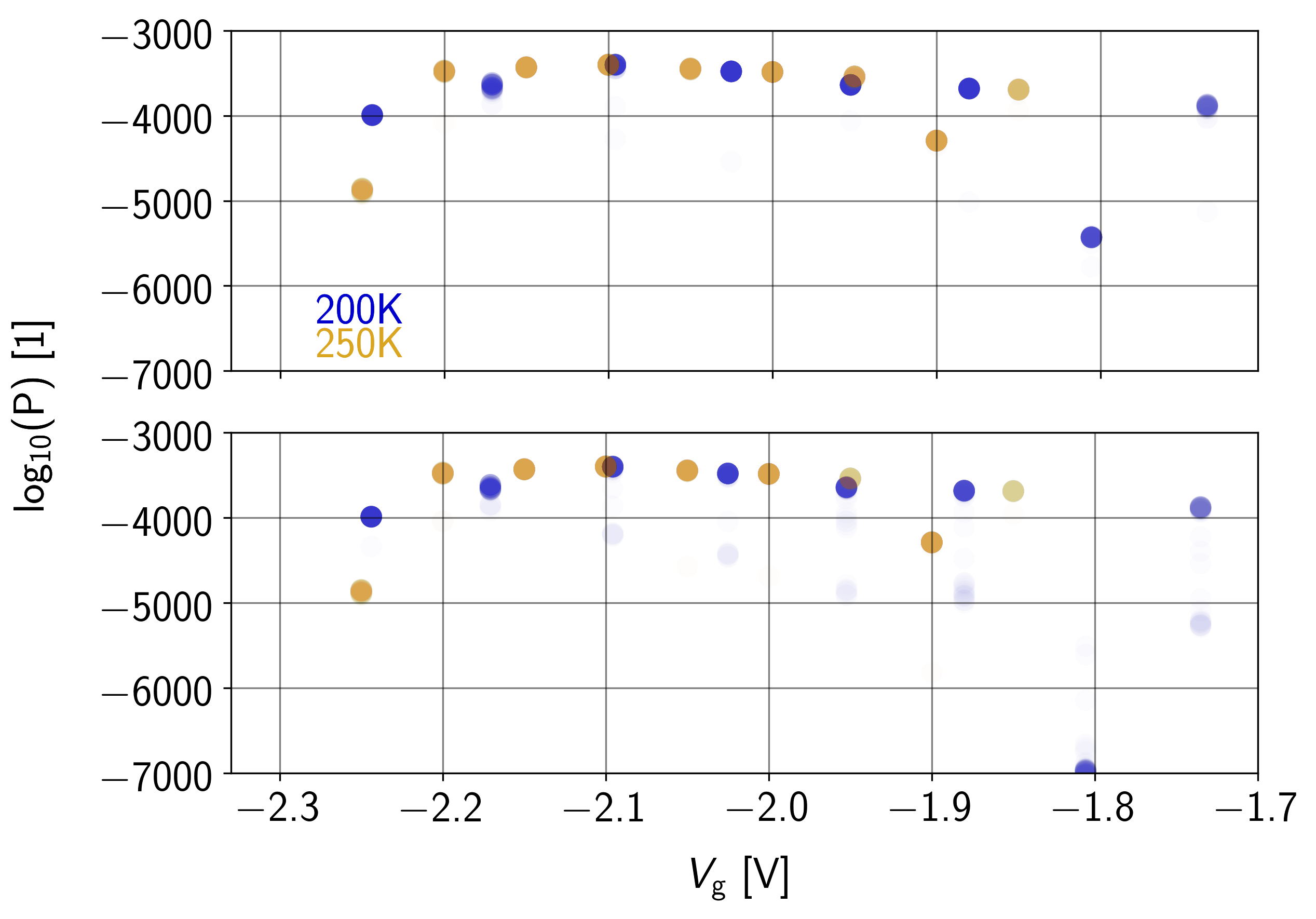
The training of the HMM was performed with the original measurement data for each temperature and bias condition using the four and five state defect structures mentioned above. Because of the dependence of the Baum-Welch algorithm presented in Section 6.7 on the initial parameters, the training was performed with seeds using Gaussian distributions for the initial step-heights as well as the initial capture and emission times. The mean values of the Gaussian distributions for capture and emission times were taken from the results in Figure 7.15.
For baseline correction, the LOWESS algorithm was chosen because of its versatility and robustness against different long-term drift patterns. After training, the results of the MAP probabilities of all data points and the corresponding step heights were examined for both defect configurations (see Figures 7.26 and 7.27). This was done primarily to check the accuracy of the extracted defect
parameters for the different voltages. It is evident that the logarithmic probabilities decrease towards the regions where  or vice versa. In the region of
  around −2.3 V, the defect is inactive most of the time and thus the number of capture and emission events is quite small, decreasing the overall accuracy.
For the other region at around −1.7 V, the emission times are much larger than the capture times. This leads to a condition where the defect is rarely in its ground state which poses another problem on top of the reduced statistics, namely the baseline correction. To catch medium-frequency signal drifts within one trace, the algorithm also needs to be set to a sensitivity where the estimated baseline can change accordingly. This however tends to pull the baseline towards the regions where the defect is in a charged state.
The extracted step heights of the defects lie between 4 mV and 5 mV with a slightly lower average value for elevated temperatures which is in line with the values given in Figure 7.16. They also possess a slight voltage dependence with decreasing values for increasing gate bias. This can probably be explained by the fact that for a stronger channel, the screening of the defect is
increased and thus its individual impact on decreases.
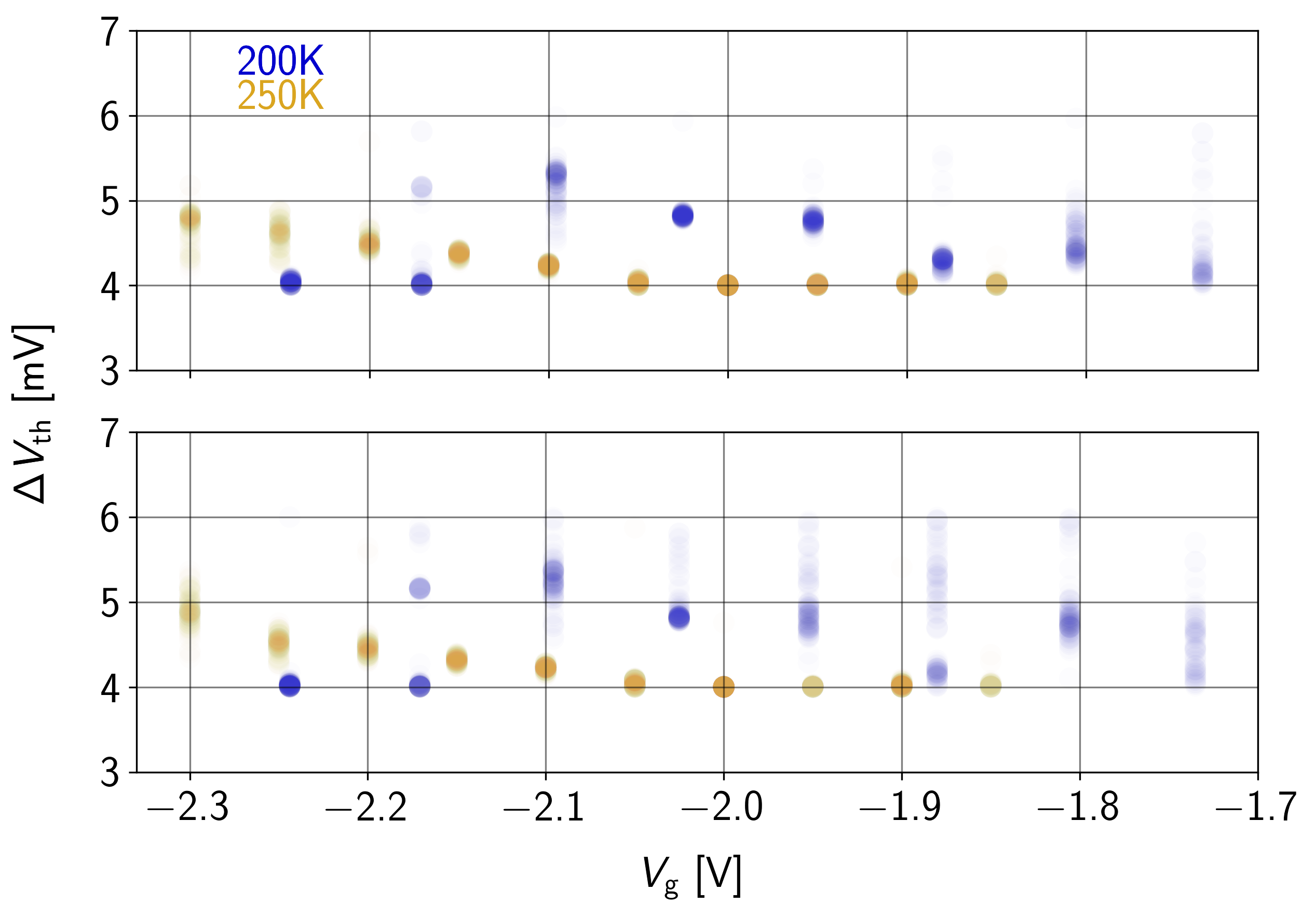
as well as their temperature dependence are in the same range like the independently obtained values in Figure 7.16, confirming the validity of the extracted parameters.
To judge which of the two defect candidates is more likely, the differences in the MAP probabilities can be plotted. If one of the defects shows a significantly higher probability across the gate voltages, this would be a strong argument in favor of the respective configuration. In Figure 7.28 the differences of the probabilities and step-heights of the five-state defect and the four-state defect are plotted.
A positive value of  thereby means that the solution for five-state defect is more likely. The differential probabilities do not show a clear trend regarding which of the two candidates is more likely to produce the measured signals although on average the five-state defect has slightly higher probabilities across many gate biases.
This could also be a consequence of the additional parameter for the HMM die to the extra state of the five-state defect. Additionally, the step height differences are pretty much centered around zero, not favoring any of the candidates. Different results in the step heights would point to a badly aligned baseline or a
significant amount of missed steps.
thereby means that the solution for five-state defect is more likely. The differential probabilities do not show a clear trend regarding which of the two candidates is more likely to produce the measured signals although on average the five-state defect has slightly higher probabilities across many gate biases.
This could also be a consequence of the additional parameter for the HMM die to the extra state of the five-state defect. Additionally, the step height differences are pretty much centered around zero, not favoring any of the candidates. Different results in the step heights would point to a badly aligned baseline or a
significant amount of missed steps.
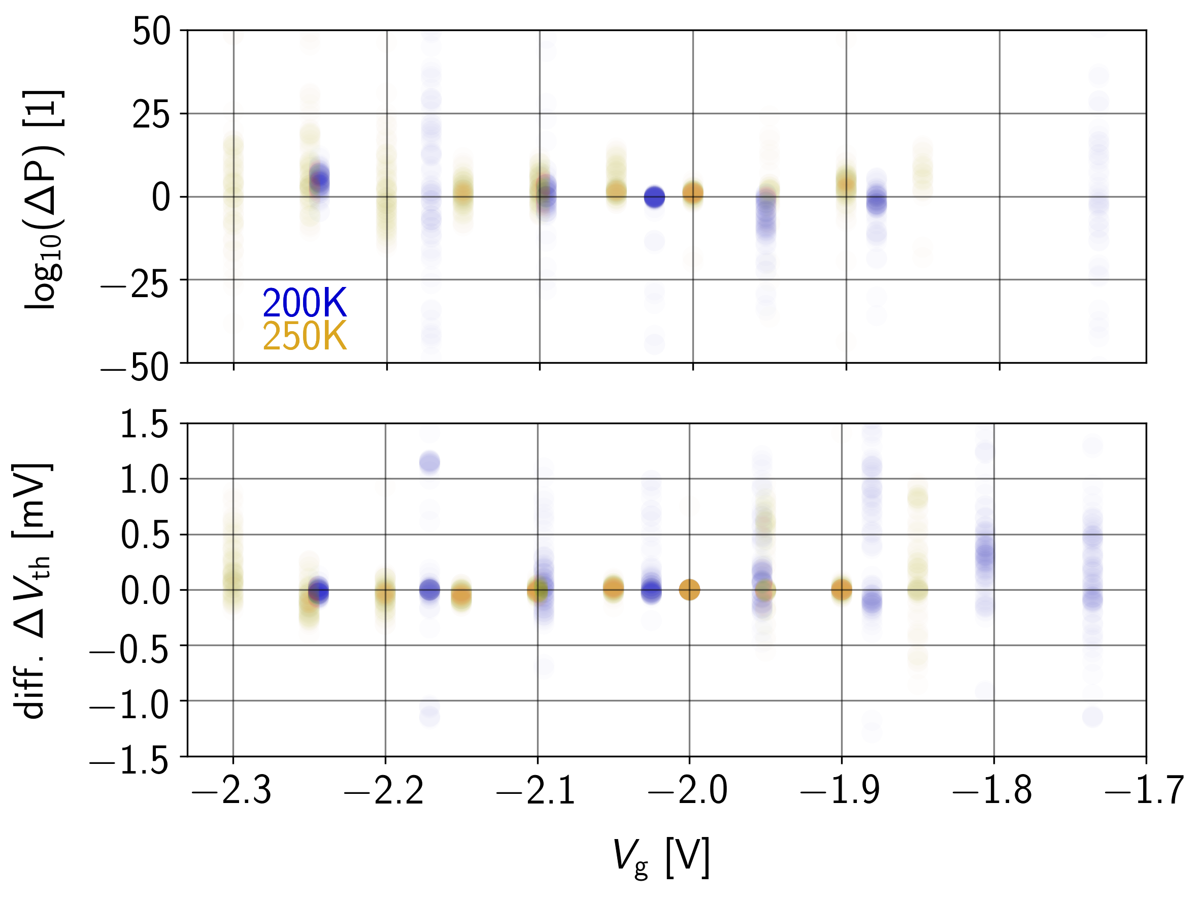
thereby means that the solution for the five-state defect is more likely. Differences in the step heights would point to a badly aligned baseline or a significant amount of missed steps. Neither of the two results show a clear tendency in favor of one of the defects, making the judgment on which of them is
more likely difficult.
Even after careful selection of the two defect candidates and evaluating their probabilities to produce the observed measurements, none of the two could be excluded so far. The last possibility left to prefer one over the other is thus the extracted time constants. The average capture and emission times were calculated from the 100 seeds using weighted averages. For the weight factors, the inverse MAP probabilities of the seeds were chosen in order to give less weight to more unlikely results.
At that point, it has to be noted that the weights are likely to overestimate unlikely training results as they were calculated using logarithmic probabilities. If on the other hand the actual probabilities had been used, most likely only a few of the seeds with the highest probability would have defined the result because the probabilities can differ by several orders of magnitude.
The extracted time constants for the four and five-state defects are plotted separately for each of the states in Figure 7.29, with the darker color being the emission time and the lighter
one being the capture time of the state. The only difference between the two defects are the transitions between states and , hence only the transitions  and
and  are affected by the additional state. Judging by the bias dependence of the extracted time constants, the five-state defect possesses a smoother, nearly exponential behavior which is typical for RTN defects. On the other hand, the transitions
  and
and  show a significant voltage dependence for
  , which normally should not be the case for thermal transitions.
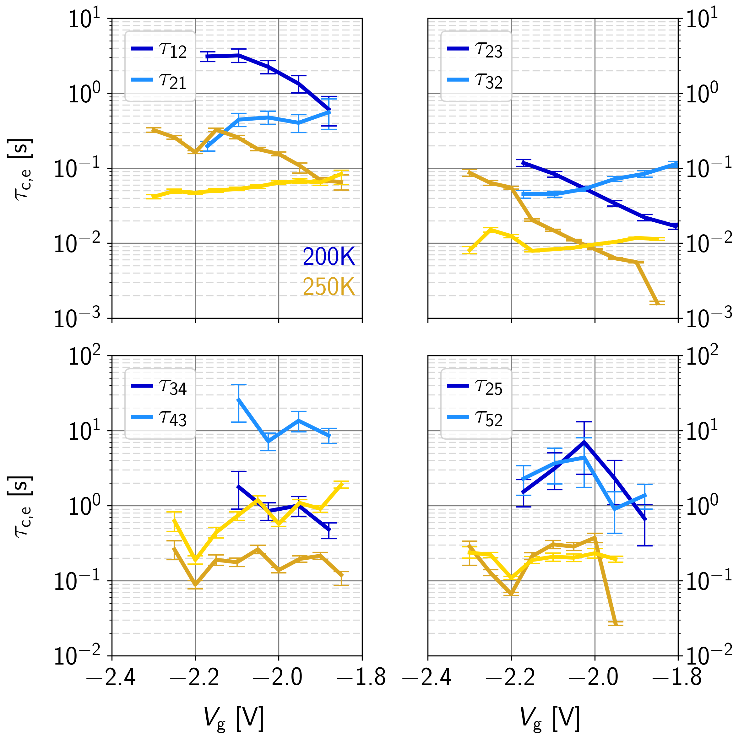
for can possibly be explained by a lack of observed transitions to this state.
As mentioned before, the measurements show only few explicit transitions pointing to a (hypothetical) state . The observed voltage dependence thus could also be caused by an insufficient number of transitions, backed by the rather large error bars for this state in Figure 7.29.
Overall, a clear tendency towards one of the proposed defect structures cannot be seen in the results. The differential probabilities in Figure 7.28 and the bias dependencies, however, make a
five-state defect structure look a bit more likely.
It should be noted at that point, that the noise-level and the associated long-term drift for the measurements at 275 K was too large for an extraction with the presented HMM library. An inspection of the resulting time constants showed almost equal capture and emission times for all states across the whole bias range. This suggests accidental fitting of measurement noise due to either a bad baseline estimation or too much noise. The MAP paths indeed revealed a lot of wrongly asserted emissions mostly due to long-term drift of the signal, and thus the results for 275 K were discarded.
Finally, a slightly modified defect parameter extraction for the trap position and the trap levels as shown in Section 7.2.3 can be done with the two defect candidates shown in
Figure 7.25. One difference is that the voltage dependence of the trap level of the double-negatively charged state is twice as high compared to that of state . Consequently, the slopes of the capture and emission barriers in (7.6) also need to be multiplied by two.
The other difference are the thermal barriers to the states and not present in the initial extraction. Those were calculated separately for capture and emission by a simple Arrhenius law for both of the states. Schematic CC diagrams for the two defect candidates are shown in Figure 7.30. Note that the relaxation energies for electron capture and emission could not be determined. Therefore, equal curvatures and distances were assumed for the potential energy surfaces in
Figure 7.30. As a consequence, the NMP barriers in this picture cannot be uniquely determined with the presented extraction methods.
The results of this extraction can be seen in Table ?? and ??. Not very surprisingly, state  closely matches defect ‘A’ in Table 7.1. The main difference here is the larger values for the defect positions, which are caused by slightly different intersection points of
the calculated time constants. The values for defect ‘B’ cannot be compared directly for two reasons. First, the defect position has to be the same which is still backed by the similar values of
closely matches defect ‘A’ in Table 7.1. The main difference here is the larger values for the defect positions, which are caused by slightly different intersection points of
the calculated time constants. The values for defect ‘B’ cannot be compared directly for two reasons. First, the defect position has to be the same which is still backed by the similar values of  in the RTN signal. Additionally, the double-negatively charged state
  by definition has twice the voltage dependence of state , which forces the extracted trap levels to be different.
In this section, single defect parameters at different cryostatic temperatures were extracted from RTN measurements on a GaN/AlGaN fin MIS-HEMT.
In Section 7.2.2, first the differences between regular fin FETs and the devices used in this work are laid out. The transfer characteristics of the measured device recorded at different temperatures are then used to calibrate the electrostatic device simulations.
The characteristic time constants of two pairs of coupled RTN producing defects are extracted in Section 7.2.3 with the spectral maps method introduced in Section 6.6.3. Additionally, important parameters like the trap level, the vertical position and the relaxation energy of the defects are extracted in Table 7.1 using a two-state NMP model.
The question if the observed signals emerge from two coupled pairs of two-state defects or a single, more complex defect structure are tried to be answered by evaluating the necessary coupling factors from RTN simulations and comparing them to those calculated for a chosen defect candidate using different methods.
In Section 7.2.4, three different approaches to estimate the short-range potential perturbation of one defect capturing a charge were explored. Based on the extracted trap level in Section 7.2.3, the most likely defect candidate was identified to be the nitrogen vacancy. Theoretical coupling factors were extracted in a worst-case sense, namely for the neighboring and the second to next neighbor nitrogen vacancies. On the other hand, HMM simulations were used to identify the required coupling factors to observe the measured coupled RTN signals. The required coupling factor of about 100 is at the upper limit of the theoretically extracted data for the nearest neighbor defect. The uncertainties in the extracted potentials, however, are quite large and enter the coupling factors exponentially. Quite interestingly, the coupling factors reported in literature closely match the values in Table 7.3 at room temperature for defects being 1 nm apart from each other.
Finally, two possible defect structures, a four-state and a five-state defect, are investigated by extracting their characteristic time constants using HMM training in Section 7.2.5. Both defect structures are compared to each other in terms of their MAP probabilities and the extracted defect distributions to find the most likely candidate. As none of them can be discarded within a reasonable likelihood, a slightly modified version of the parameter extraction introduced in Section 7.2.3 is carried out for both defect structures (see Table ?? and ??).


![(7.5) \{begin}{align} \frac {\partial }{\partial V_\mathrm {g}}\Big [\ln (1) - \ln (\tauce )\Big ] = & \frac {\partial }{\partial {V_\mathrm {g}}} \Big [\ln (\sigma ) -\frac {\mathcal {E}_{c,e}}{\kb T}\Big ]\notag \\[1em] \kb
T\frac {\partial \ln (\tauce )}{\partial V_\mathrm {g}} = & \frac {\partial \mathcal {E}_{c,e}}{\partial V_\mathrm {g}} \eqlabel {arrheniusdVg} \{end}{align}](images/image-878.svg)


![(7.18) \begin{equation} \lvert E(r)\rvert = \frac {q_\mathrm {0}}{4\pi \varepsilonup _\mathrm {0}\varepsilon _\mathrm {r}r^3} \left [1-\exp \left ({-\frac {2r}{r_\mathrm {c}}}\right )\left (1+\frac {2r}{r_\mathrm {c}}+\frac
{2r^2}{r_\mathrm {c}^2}\right )\right ] \eqlabel {hydrogen_E} \end{equation}](images/image-923.svg)
![(7.19) \begin{equation} \varphi (r) = \frac {q_\mathrm {0}}{4\pi \varepsilonup _\mathrm {0}\varepsilon _\mathrm {r}} \left [ \frac {\exp \left (\displaystyle {-\frac {2r}{r_\mathrm {c}}}\right )-1}{r}+\frac {\exp \left
(\displaystyle {-\frac {2r}{r_\mathrm {c}}}\right )}{r_\mathrm {c}}\right ] \eqlabel {hydrogen_phi} \end{equation}](images/image-924.svg)