Charges trapped at distinct microscopic defect sites naturally affect their local surroundings. As such, the process of charge exchange with some reservoir always causes the defect site to be deformed due to the change in the local potential surface and a subsequent relaxation towards the new thermal equilibrium [120]. Early applications of the NMP theory were dedicated to the modeling of deep levels in semiconductors [121–124]. The modeling of transient  drift with NMP transitions to oxide defects was first done by Tewksbury [125, 126].
This section briefly only summarizes the most important concepts of the NMP theory and its applications for describing the transient drift of devices. A more elaborate discussion on the NMP theory including the discussion of different BTI models can be found in [88]. Details on the derivation of the NMP model in the context of charge transitions to oxide defects
are given in [86].
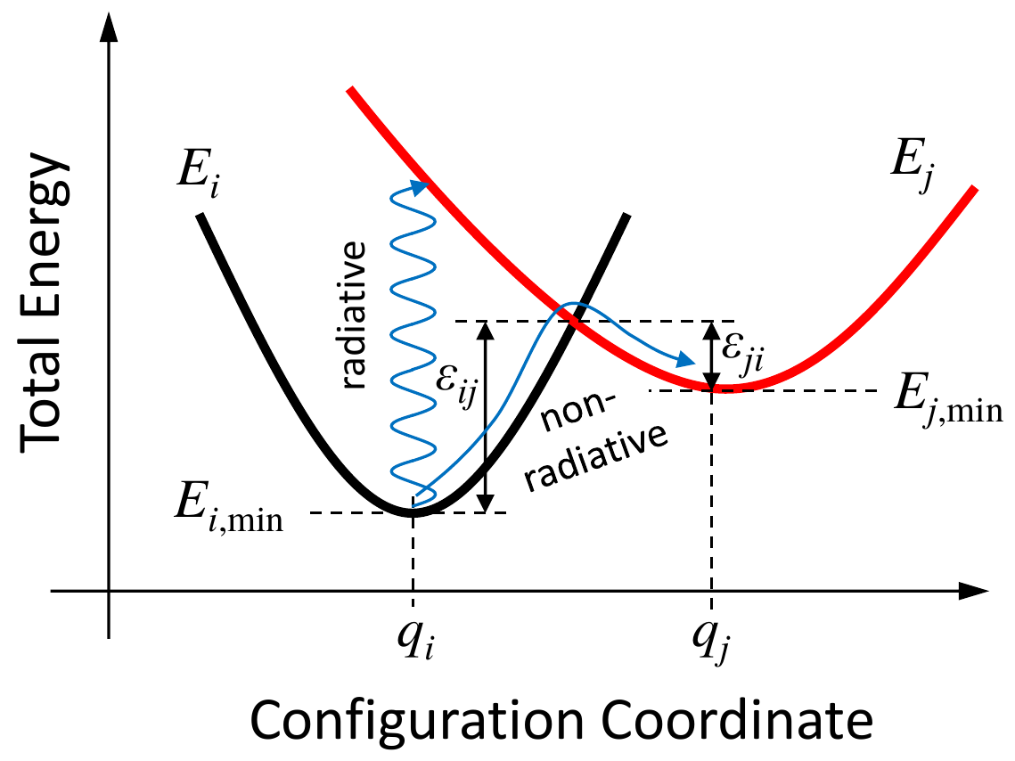
Charge transitions between two states (i.e., the defect state and some reservoir) can in general either happen directly (radiative) or phonon-assisted (non-radiative). The physics of these transitions is governed by electron-phonon coupling which describes the coupling between the wave functions for the system of electrons and phonons. The solution of the two coupled Schrödinger equations is, however, unfeasible for all practical purposes. This problem can be circumvented by taking advantage of the fact that the motions of electrons is usually much faster than the motion of phonons. The so-called Born-Oppenheimer approximation [127] allows solving the two systems separately from each other.
The electron wave functions can thus be obtained for the Coulomb energies of the fixed nuclei positions leading to a  -dimensional potential energy surface for a system of
  atoms. By taking into account that transitions between two states of the potential energy surface are most likely to happen across the minimum-energy path, this multidimensional surface can be reduced to a so-called CC diagram describing the dominant transition path between two states (see
Figure 5.3). Even though the shape of the energy surface in the CC diagram can theoretically be derived from first-principle simulations [128] for
certain defect candidates, the solution of the resulting non-analytic quantum systems is still cumbersome.
atoms. By taking into account that transitions between two states of the potential energy surface are most likely to happen across the minimum-energy path, this multidimensional surface can be reduced to a so-called CC diagram describing the dominant transition path between two states (see
Figure 5.3). Even though the shape of the energy surface in the CC diagram can theoretically be derived from first-principle simulations [128] for
certain defect candidates, the solution of the resulting non-analytic quantum systems is still cumbersome.
Only the approximation of the actual potential energy surface in the CC diagram by quantum harmonic oscillators allows for an analytic treatment of the problem. The total energy of a system being in state  with the minimum energy
  at the equilibrium position
  and the curvature
  reads
reads
The transition rate in the harmonic approximation can be derived from the carrier distribution function  and the density of states
  in the reservoir, the electronic matrix element
  and the lineshape function
  [125]:
The electronic matrix element thereby accounts for elastic tunneling of electrons from the reservoir to the defect site. The lineshape function accounts for the overlaps between the initial and final vibrational states of the system and can be calculated from the Franck-Condon factors [86, 129, 130].
There is convincing evidence that phonon-assisted transitions play an important role in charge trapping events in oxide defects. Since thermal emission into the conduction or valence bands at the defect site is typically unfeasible, tunneling of carriers from the channel (or the gate) to the defect site is indispensable. If elastic tunneling was the dominant process, the measured time constants should possess certain properties, all of which are contradicted by existing measurement data [88]:
• The measured temperature activation of the time constants is measured to be Arrhenius-like whereas for pure elastic tunneling the temperature dependence is distinctively weak [131].
• The time constants of devices with thin oxides would have to be tunnel-limited which is in contradiction to measurements done for thin oxides [132].
• Defects closer to the channel would have smaller time constants and thus would be charged first. This mechanism implies a correlation between the trap positions extracted from single-defect measurements, usually obtained from the intersection between  and
and  , and the capture times which could not be found experimentally [133].
• The time constants should have a nearly linear bias dependence; single defect studies however revealed a more complex behavior [116].
The examples above thus show that phonon interactions have to be an integral part of a physics-based model for BTI.
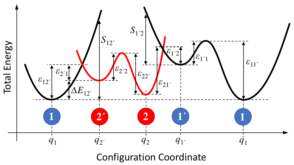
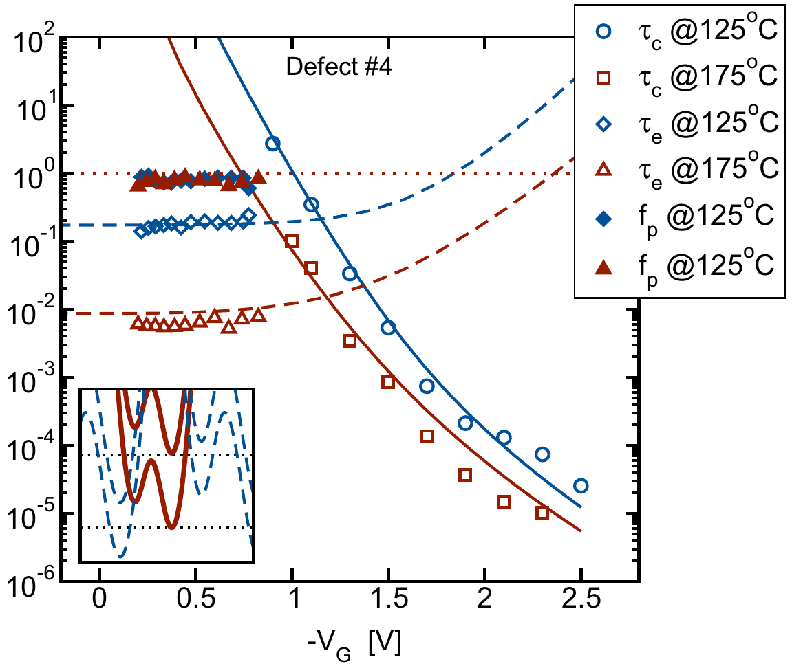
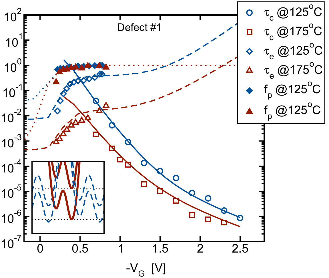
The NMP four-state model emerged from one of the first models which used NMP transitions for the description of charge trapping in oxide defects called the two-stage model [134]. The two-stage model already allowed to model defects producing anomalous RTN by using a three-state NMP model with one meta-stable state. The development of the four-state model was driven by single defect TDDS measurements in ultra-scaled silicon p-MOS devices which revealed two distinct types of oxide defects which were named fixed oxide defects and switching oxide defects. While fixed oxide traps possess a nearly constant bias dependence, switching oxide traps show a distinct bias dependency of the emission times for lower gate voltages (see Figure 5.4). These switching type of defects were also consistent with other single-defect observations like anomalous or temporary RTN.
The NMP four-state model has already proven to successfully describe charge trapping in advanced silicon technology [AGC3][88, 135, 136], but also other advanced technologies like SiGe [AGJ3, AGJ4, AGC4], GaN [AGC1], and various two-dimensional materials [AGJ5][137–139].
By combining first principle simulations with the defect parameters extracted from different measurements, several different defect candidates having the proper structure to fulfill all the requirements of the four-state NMP model in SiO2 could be identified [86, 128]. Each of the four states thereby links to a specific atomic configuration and charge state. As an example, Figure 5.5 shows one of these defect candidates, the  center. The bias-dependent switching oxide transition path goes from state
  to
to  to
to  , whereas the fixed oxide defect path would be from to
  to .
to .
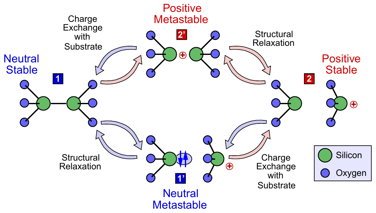
center as an example for a four-state defect with its two stable states and and its two metastable states and . The four states offer two distinct pathways for fixed oxide (over ) and switching oxide (over ) defects (from [110]).
The schematic CC diagram for a defect similar to the one shown in Figure 5.5 can be found in Figure 5.6. The
NMP transition barriers  in the classical limit can be calculated directly from the intersection point of the two parabolas defined according to (5.7).
Because of the transitions over lower energy barriers being dominant, the positive sign of the square root in (5.9) can be neglected. The equation can be rewritten using common definitions for the the energy differences  , relaxation energy
  and the curvature ratios
  ,
,
which for  leads to
The singularity for  can be removed and the transition barrier then reads
Note that the trap levels and are field dependent with the energy shift being proportional to the trap position  in a constant field approximation.
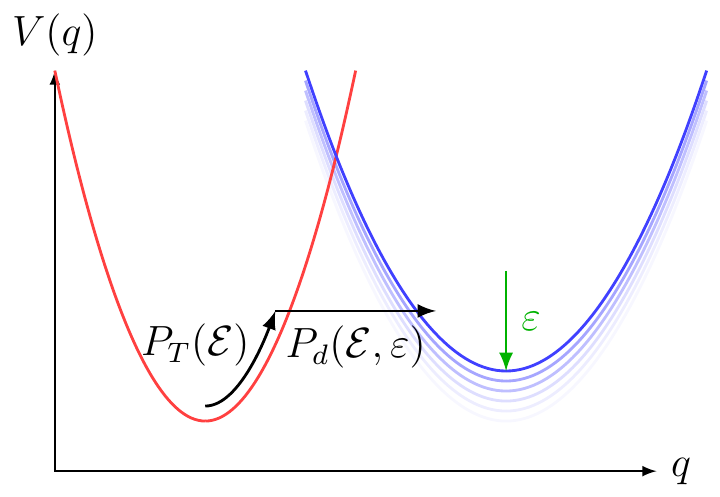
In the classical limit, the energy has to be overcome for a NMP transition to happen. Boltzmann statistics gives the probability of the vibrational system to be excited by this energy, and thus the transition rate and thus (5.8) can be calculated to
The thermal transition rates to the metastable states without charge transfer can simply be modeled by an Arrhenius law with the activation energy and the attempt frequency  as
as
Further simplifications can be done if instead of the NMP transitions happening to a band of states as depicted in (5.8), only the band edges of the conduction and valence band of the reservoir are considered. This makes the
transition barrier and the electronic matrix element independent of energy and thus they can be moved out of the integral. Furthermore, the distribution function in equilibrium conditions can be identified as the Fermi-Dirac distribution and with  , the reverse rate is linked to the forward rate by:
If the integral in (5.16) and the NMP barriers are split up for the conduction and valence band, in the hole picture of Figure 5.6 one obtains
The remaining integrals can easily be identified as the electron and hole concentrations respectively. As mentioned earlier, the electronic matrix element accounts for elastic tunneling of the carriers. The electronic matrix element can be calculated by multiplying the tunneling probability  with a capture cross-section
  and a thermal velocity
  of the carriers. Furthermore, the process is assumed to be symmetrical so that
  .
.
The tunneling probabilities could be theoretically derived from the Schrödinger equation. However, the potential well around the defect site and thus the electronic wave function of the defect can hardly be determined. Therefore, the WKB approximation [140] is often used to calculate analytically for different shapes of the energy barriers.
The most important energy barriers for BTI are the trapezoidal and the triangular barrier depicted in Figure 5.7. With the carrier energy  , the elementary charge
  and the effective tunnel mass
  , the equation for a trapezoidal barrier reads [141, 142]:
For the special case of a triangular barrier, the equation simplifies to:
When putting all of the above together, the expressions for the NMP rates can finally be approximated with:
Note that in Figure 5.6, the (gate voltage dependent) trap level corresponds to  and
and  is the conduction or valence band edge of the reservoir and the calculation of the NMP barriers in (5.13) needs to be adapded accordingly. Additionally, the NMP barriers for the forward and backward transitions
are not independent from each other and can be calculated from
is the conduction or valence band edge of the reservoir and the calculation of the NMP barriers in (5.13) needs to be adapded accordingly. Additionally, the NMP barriers for the forward and backward transitions
are not independent from each other and can be calculated from  .
.
The rates derived in (5.27)-(5.30) can be used to calculate the NMP transition rates for all kinds of defects, as long as their
positions and CC diagrams are known. In large-area devices with many different pre-existing defects, the total BTI degradation can be modeled in a Monte Carlo fashion, which means distributing the main defect parameters like , , and around a their mean values using probability distributions.
In real devices different types of defects exist alongside each other, each one having a certain structure and number of states. On top of that, the amorphous nature of oxides will inevitably lead to random fluctuations of the NMP parameters for each of those defect types. The resulting set of CC diagrams and eventual correlations between different NMP parameters thus can hardly be determined at all. Because of that, the Monte Carlo sampling of the four-state model is usually done on a set of independent and normally distributed parameters [135].
The average number of defects can easily be calculated from the assumed defect concentration within the oxide. Their random fluctuations are commonly thought to follow a Poisson distribution given by [143, 144]
The electrostatic impact of each defect based on its position within the oxide can be estimated using a simple one-dimensional charge sheet approximation. Alternatively, the defect charges can simply be entered to the right-hand side of the Poisson equation in electrical device simulators.
Unlike the NMP two-stage model, the four-state model does not include any mechanism for the creation and passivation of defects. Thus it is limited to pre-existing defects in the oxide commonly attributed to the recoverable part of BTI. A number of studies however propose a coupled mechanism of creation and annihilation of defect sites driven by the relocation of hydrogen [145, 146]. This triggered another evolution of the NMP four-state model called the gate-sided hydrogen release model [147]. The mechanisms covered by this model are very specifically designed for the Si/SiO2 interface and therefore beyond the scope of this work.
Within the framework of the NMP theory, defects can interact not only with a single but with an arbitrary number of charge reservoirs (usually the transistor channel and the gate). Thus, the NMP model can also be extended to investigate TAT and SILC in MOSFETs and flash memory devices [AGT1][148–151].
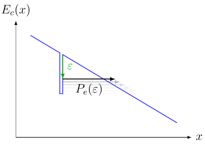
For most BTI defects, the charge exchange is governed by elastic tunneling from the charge reservoir (gate or channel) followed by a phonon-assisted transition, see (5.8). This, however, omits two additional exchange paths, namely the conduction and the valence bands at the site of the defect. Neglecting these rates is a valid approach for insulators as the ionization energies from the trap level to the local band edges are usually very large and the density of electrons and holes are rather low. For shallow defects in semiconductors or high fields, the local band rates can be of relevance, however. As an example, in Figure 5.8 all possible charge exchange paths of a defect in the barrier of a GaN/AlGaN HEMT with a Schottky gate are shown.

For emissions to the local bands at the site of the trap, no electron tunneling is required. Therefore the electronic matrix element in (5.24) is evaluated for  and thus a constant. Because of the transition taking place locally, the implicit field dependence of the NMP barriers vanishes so that the transition barriers are constant and independent of the field. At higher fields, non-local transitions with tunneling to neighboring bands can become more favorable
compared to pure thermal excitations.
and thus a constant. Because of the transition taking place locally, the implicit field dependence of the NMP barriers vanishes so that the transition barriers are constant and independent of the field. At higher fields, non-local transitions with tunneling to neighboring bands can become more favorable
compared to pure thermal excitations.
The charge transition mechanism can again be split into three parts, the thermal excitation probability  , the NMP transition probability
  and the tunneling probability
  , see Figure 5.9. In that case, the rates can be split into a field-dependent and a field-independent part:
The field-independent part of the rates can be calculated by (5.27)-(5.30) with  . Note that for this transition, the NMP barrier is also independent of the applied field. When band-bending in the semiconductor can be neglected (i.e., the electric field across the semiconductor can be assumed constant), the field-dependent part is calculated by taking into account elastic tunneling through
a triangular barrier. For each infinitesimal barrier lowering, an additional amount of states can be reached. The product of effective density of states, lineshape function and electronic matrix element must then be summed over the barrier lowering
. Note that for this transition, the NMP barrier is also independent of the applied field. When band-bending in the semiconductor can be neglected (i.e., the electric field across the semiconductor can be assumed constant), the field-dependent part is calculated by taking into account elastic tunneling through
a triangular barrier. For each infinitesimal barrier lowering, an additional amount of states can be reached. The product of effective density of states, lineshape function and electronic matrix element must then be summed over the barrier lowering  . With the lowered barrier
  , the field dependent rates for holes are given by [AGT1]:
The differentials for electrons and holes in (5.33)-(5.36) stand for the additional number of states that can be reached due to an
infinitesimal barrier-lowering. By assuming that the lowest point of the integration is still well above the Fermi level (i.e., by assuming Boltzmann distributions) and with the additional amount of electrons and holes can be calculated as
Inserting the expressions for the number of electrons and holes yields [AGT1]
With similar simplifications for the lineshape function and the electronic matrix element as explained in Section 5.2.2, the final rates for the interaction with the local bands can be expressed as [AGT1]:
There, the NMP barriers  and
and  are the field-dependent transition energies calculated from
  and
and  or
or  respectively. In general, transitions to the local bands only contribute significantly to the overall NMP rates if the trap level is shallow or if the fields are very high. This model can be used as a more physical alternative to other TAT models like for example the Frenkel-Poole model [152] used to calculate barrier leakage currents in GaN/AlGaN HEMTs. Another benefit of this model is its seamless transition from a regime dominated by Fowler-Nordheim tunneling [141] into a regime where the defect properties dominate the tunneling currents [41, 42].